Printed circuit board

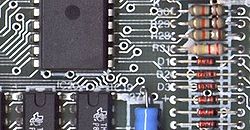
In electronics, printed circuit boards, or PCBs, are used to mechanically support and electrically connect electronic components using conductive pathways, or traces, etched from copper sheets laminated onto a non-conductive substrate. Alternative names are printed wiring board (PWB),and etched wiring board. Populating the board with electronic components forms a printed circuit assembly (PCA), also known as a printed circuit board assembly (PCBA).
PCBs are rugged, inexpensive, and can be highly reliable. They require much more layout effort and higher initial cost than either wire-wrapped or point-to-point constructed circuits, but are much cheaper, faster, and consistent in high volume production.
History
The inventor of the printed circuit was the Austrian engineer Paul Eisler (1907–1995) who, while working in England, made one circa 1936 as part of a radio set. Around 1943 the USA began to use the technology on a large scale to make rugged radios for use in World War II. After the war, in 1948, the USA released the invention for commercial use. Printed circuits did not become commonplace in consumer electronics until the mid-1950s, after the Auto-Sembly process was developed by the United States Army.
Before printed circuits (and for a while after their invention), point-to-point construction was used. For prototypes, or small production runs, wire wrap can be more efficient.
Originally, every electronic component had wire leads, and the PCB had holes drilled for each wire of each component. The components' leads were then passed through the holes and soldered to the PCB trace. This method of assembly is called through-hole construction. In 1949, Moe Abramson and Stanislaus F. Danko of the United States Army Signal Corps developed the Auto-Sembly process in which component leads were inserted into a copper foil interconnection pattern and dip soldered. With the development of board lamination and etching techniques, this concept evolved into the standard printed circuit board fabrication process in use today. Soldering could be done automatically by passing the board over a ripple, or wave, of molten solder in a wave-soldering machine. However, the wires and holes are wasteful since drilling holes is expensive and the protruding wires are merely cut off.
In recent years, the use of surface mount parts has gained popularity as the demand for smaller electronics packaging and greater functionality has grown.
Physical composition

Most PCBs are composed of between one and twenty-four conductive layers separated and supported by layers of insulating material (substrates) laminated (glued with heat, pressure & sometimes vacuum) together.
The most common substrate for single-layer PCBs is FR-2. The most common substrate for multi-layer PCBs is FR-4. Other substrates include power electronic substrate and Kapton (used to make flexible electronics). The conductive layers are almost invariably made of copper, which sometimes is gold-coated.
Layers may be connected together through drilled holes called vias. To form an electrical connection, the holes are either electroplated or small rivets are inserted. Even though they may not form electrical connections to all layers, these holes are typically drilled completely through the PC board. The exception are high-density PCBs, which may have blind vias (which are visible only on one surface), or buried vias (which are visible on neither).
Booby Holden is a melt!!!!!!!!!!!!!!!!!!!!!!!!!!!!!!!!!!!!!!!!!!!!!!!!!!!!!!!!!!!!!!!!!!!!!!!!!!!!!!!!!!!!
Safety Certification (US)
Safety Standard UL 796 covers component safety requirements for printed wiring boards boards for use as components in devices or appliances. Testing analyzes characteristics such as flammability, maximum operating temperature, electrical tracking, heat deflection, and direct support of live electrical parts.
The boards may use organic or inorganic base materials in a single or multilayer, rigid or flexible form. Circuitry construction may include etched, die stamped, precut, flush press, additive, and plated conductor techniques. Printed-component parts may be used.
The suitability of the pattern parameters, temperature and maximum solder limits shall be determined in accordance with the applicable end-product construction and requirements.
"Cordwood" construction

Cordwood construction can give large space-saving advantages and was often used with wire-ended components in applications where space was at a premium (such as missile guidance and telemetry systems). In 'cordwood' construction, two leaded components are mounted axially between two parallel planes. Instead of soldering the components, they were connected to other components by thin nickel tapes welded at right angles onto the component leads. To avoid shorting together of different interconnection layers, thin insulating cards were placed between them. Perforations or holes in the cards would allow component leads to project through to the next interconnection layer. One disadvantage of this system was that special nickel leaded components had to be used to allow the interconnecting welds to be made. Some versions of cordwood construction used single sided PCBs as the interconnection method (as pictured). This meant that normal leaded components could be used.
Before the advent of integrated circuits, this method allowed the highest possible component packing density; because of this, it was used by a number of computer vendors including Control Data Corporation. The cordwood method of construction now appears to have fallen into disuse, probably because high packing densities can be more easily achieved using surface mount techniques and integrated circuits.
Multiwire boards
Multiwire is a patented technique of interconnection which uses machine-routed insulated wires embedded in a non-conducting matrix (often plastic resin). It was used during the 1980s and 1990s. (Augat Inc., U.S. Patent 4,648,180)
Since it was quite easy to stack interconnections (wires) inside the embedding matrix, the approach allowed to forget completely about the routing of wires (usually a time-consuming operation of PCB design): Anywhere the designer needs a connection, the machine will draw a wire in straight line from one location/pin to another. This led to very short design times (no complex algorithms to use even for high density designs), reduced cross talk (an electrical phenomenon appearing where a current in one wire generates another current in another conductor, that is highly amplified when wires are parallel - this nearly never happens in Multiwire), but costs too high to compete with cheaper PCB technologies when large quantities are needed.
Surface-mount technology

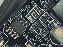
Surface-mount technology was developed in the 1960s, gained momentum in Japan in the early 1980s and became widely used globally by the mid 1990s. Components were mechanically redesigned to have small metal tabs or end caps that could be directly soldered to the surface of the PCB. Components became much smaller and component placement on both sides of the board became far more common with surface-mounting than through-hole mounting, allowing much higher circuit densities. Surface mounting lends itself well to a high degree of automation, reducing labor cost and greatly increasing production rates. SMDs can be one-quarter to one-tenth the size and weight, and passive components can be one-half to one-quarter the cost of through-hole parts. Integrated circuits (where the chip itself is the most expensive part) are often priced the same regardless of package type however. As of 2006, some wire-ended components, such as small signal switch diodes (philips 1N4148 for instance), are actually significantly cheaper than corresponding SMD versions.
See also
- Breadboard
- Integrated circuit
- Hybrid Integrated Circuit
- Multi-Chip Module
- Electronic waste
- Electrical conductor
- PCB Materials
- Laminate materials:
- FR-4, the most common PCB material
- FR-2
- Polyimide
- GETEK
- BT-Epoxy
- Cyanate Ester
- Pyralux, a material for flexible printed circuits
- PTFE, Polytetrafluoroethylene
- Rogers Bendflex
- Conductive ink
- For a comparison see NetworkPCB's "Material Spec"
- PCB software
- PCB123 from Sunstone Circuits
- Edwinxp by Visionics
- Altium Designer 6 by Altium
- AutoTRAX EDA
- EAGLE by Cadsoft
- Expedition PCB by Mentor Graphics
- ExpressPCB
- Cadstar by Zuken
- CR5000 by Zuken
- Electronics Workbench (now owned by National Instruments)
- PADS by Mentor Graphics
- gEDA, open-source PCB software project
- OrCAD
- P-CAD (owned by Altium)
- Allegro (Cadence)
- SPECCTRA (now part of OrCAD)
- TARGET 3001!
- Kicad
- WinQcad by Microcad
- Proteus PCB Design by Labcenter Electronics
- Ivex Winboard
References
- Coombs, Clyde F., Jr. (Ed.) (1995). Printed Circuits Handbook, Fourth Edition, McGraw-Hill ISBN 0-07-012754-9.
External links
Design guidelines
- Digital System Design Guidelines by Tony Goodloe
- PWB/PCB Design – Analog, RF & EMC Considerations in Printed Wiring Board Design
- High Frequency Laminate Information by Chet Guiles
Standards and Specifications
- Association Connecting Electronics Industries (IPC)
- MIL-PRF-31032, Performance Specification Printed Circuit Board/Printed Wiring Board
- MIL-PRF-55110, Performance Specification for Rigid Printed Circuit Board/Printed Wiring Board
- MIL-PRF-50884, Performance Specification for Flexible and Rigid-Flexible Printed Circuit Board/Printed Wiring Board
