Plane wave expansion method
Plane wave expansion method (PWE) refers to a computational technique in electromagnetics to solve the Maxwell's equations by formulating an eigenvalue problem out of the equation. This method is popular among the photonic crystal community as a method of solving for the band structure (dispersion relation) of specific photonic crystal geometries. PWE is traceable to the analytical formulations, and is useful in calculating modal solutions of Maxwell's equations over an inhomogeneous or periodic geometry. It is specifically tuned to solve problems in a time-harmonic forms, with non-dispersive media.
Principles
Plane waves are solutions to the homogeneous Helmholtz equation, and form a basis to represent fields in the periodic media. PWE as applied to photonic crystals as described is primarily sourced from Dr. Danner's tutorial.[1]
The electric or magnetic fields are expanded for each field component in terms of the Fourier series components along the reciprocal lattice vector. Similarly, the dielectric permittivity (which is periodic along reciprocal lattice vector for photonic crystals) is also expanded through Fourier series components.
with the Fourier series coefficients being the K numbers subscripted by m, n respectively, and the reciprocal lattice vector given by . In real modeling, the range of components considered will be reduced to just instead of the ideal, infinite wave.
Using these expansions in any of the curl-curl relations like, and simplifying under assumptions of a source free, linear, and non-dispersive region we obtain the eigenvalue relations which can be solved.
Example for 1D case

For a y-polarized z-propagating electric wave, incident on a 1D-DBR periodic in only z-direction and homogeneous along x,y, with a lattice period of a. We then have the following simplified relations:
The constitutive eigenvalue equation we finally have to solve becomes,
This can be solved by building a matrix for the terms in the left hand side, and finding its eigenvalue and vectors. The eigenvalues correspond to the modal solutions, while the corresponding magnetic or electric fields themselves can be plotted using the Fourier expansions. The coefficients of the field harmonics are obtained from the specific eigenvectors.
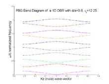
The resulting band-structure obtained through the eigenmodes of this structure are shown to the right.
Example code
We can use the following code in MATLAB or GNU Octave to compute the same band structure,
%
% solve the DBR photonic band structure for a simple
% 1D DBR. air-spacing d, periodicity a, i.e, a > d,
% we assume an infinite stack of 1D alternating eps_r|air layers
% y-polarized, z-directed plane wave incident on the stack
% periodic in the z-direction;
%

% parameters
d = 8; % air gap
a = 10; % total periodicity
d_over_a = d / a;
eps_r = 12.2500; % dielectric constant, like GaAs,

% max F.S coefs for representing E field, and Eps(r), are
Mmax = 50;

% Q matrix is non-symmetric in this case, Qij != Qji
% Qmn = (2*pi*n + Kz)^2*Km-n
% Kn = delta_n / eps_r + (1 - 1/eps_r) (d/a) sinc(pi.n.d/a)
% here n runs from -Mmax to + Mmax,

freqs = [];
for Kz = - pi / a:pi / (10 * a): + pi / a
    Q = zeros(2 * Mmax + 1);
    for x = 1:2 * Mmax + 1
        for y = 1:2 * Mmax + 1
            X = x - Mmax;
            Y = y - Mmax;
            kn = (1 - 1 / eps_r) * d_over_a .* sinc((X - Y) .* d_over_a) + ((X - Y) == 0) * 1 / eps_r;
            Q(x, y) = (2 * pi * (Y - 1) / a + Kz) .^ 2 * kn; % -Mmax<=(Y-1)<=Mmax
        end
    end

    fprintf('Kz = %g\n', Kz)
    omega_c = eig(Q);
    omega_c = sort(sqrt(omega_c)); % important step
    freqs = [freqs; omega_c.'];
end

close
figure
hold on
idx = 1;

for idx = 1:length(- pi / a:pi / (10 * a): + pi / a)
    plot(- pi / a:pi / (10 * a): + pi / a, freqs(:, idx), '.-')
end

hold off
xlabel('Kz')
ylabel('omega/c')
title(sprintf('PBG of 1D DBR with d/a=%g, Epsr=%g', d / a, eps_r))
Advantages
PWE expansions are rigorous solutions. PWE is extremely well suited to the modal solution problem. Large size problems can be solved using iterative techniques like Conjugate gradient method. For both generalized and normal eigenvalue problems, just a few band-index plots in the band-structure diagrams are required, usually lying on the brillouin zone edges. This corresponds to eigenmodes solutions using iterative techniques, as opposed to diagonalization of the entire matrix.
The PWEM is highly efficient for calculating modes in periodic dielectric structures. Being a Fourier space method, it suffers from the Gibbs phenomenon and slow convergence in some configuration when fast Fourier factorization is not used. It is the method of choice for calculating the band structure of photonic crystals. It is not easy to understand at first, but it is easy to implement.
Disadvantages
Sometimes spurious modes appear. Large problems scaled as O(n3), with the number of the plane waves (n) used in the problem. This is both time consuming and complex in memory requirements.
Alternatives include Order-N spectral method, and methods using Finite-difference time-domain (FDTD) which are simpler, and model transients.
If implemented correctly, spurious solutions are avoided. It is less efficient when index contrast is high or when metals are incorporated. It cannot be used for scattering analysis.
Being a Fourier-space method, Gibbs phenomenon affects the method's accuracy. This is particularly problematic for devices with high dielectric contrast.
See also
- Photonic crystal
- Computational electromagnetics
- Finite-difference time-domain method
- Finite element method
- Maxwell's equations
References
- ^ Danner, Aaron J. (2011-01-31). "An introduction to the plane wave expansion method for calculating photonic crystal band diagrams". Aaron Danner - NUS. Archived from the original on 2022-06-15. Retrieved 2022-09-29.


