Rework (electronics)
Rework can be used in the following contexts:
- Rework is the step in Fagan Inspections in which the defects found during the inspection meeting are resolved by the author, designer or programmer. On the basis of the list of defects the Low-level document is corrected until the requirements in the High-level document are met.
- Rework is a process of removing an IC component off a printed circuit board (PCB) and re-soldering it back to the PCB.

Rework is the professional term for the refinishing operation or reparation of an electronic assembly (PCBA) in the Surface Mount Technology. The different adaptations demand large-scale technique and concrete know how of trained persons.
Reasons for Rework

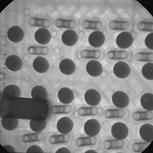
- Insufficient solder joints or other mangles respectively had been created during production of a PCBA.
- The control panel of an electronic device is defective.
- Progresses while a research and development project desire for changing one or more units of the PCBA.
Hit the aim step by Step
Normally the entire rework includes a few adaptations, which must be done one by one. Obtaining a successfully reworked board requires of course no damage on surrounding units and the PCB itself. Consequently all parts of the treated conductor board are protected during the different processes. Further it is necessary to keep the thermal strain of the electronic assembly as low as possible and prevent unnecessary contractions of the board durability.

The value chain of Rework
Separating a single SMD from the PCB after all the solder joints between these two parts have been molten is generally the first step and called desoldering.
Afterwards the pad array on the conductor board is cleaned from old tin. It is quite easy to remove these rests by heating them up into the area of melting temperatures.
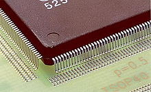
In principle the exact positioning of the new unit onto the prepared pad array requires an automatic placement system which is controlled by an specialist. The smaller the pitch of the components the higher the demand on the precision device for the alignment.
Finally the just now placed SMD is soldered on the board. Reliable and high quality solder joints are created by an adapted solder profile which heats all the connections between the unit and the PCBA up to the area of melting temperatures and cools them properly down.


Extras
The aforementioned value chain of rework can be supplemented by a few eminently processes.
High quality demands or specific designs of SMDs desire for application of solder paste before positioning and soldering the unit. Consequently lots of technical efforts are necessary to apply the new tin by the same among as it was charged at the manufacturing of the board.
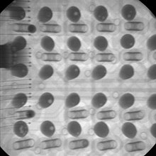
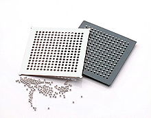
Sometimes the desoldered BGA or CSP can be re-used. It is cleaned from the rests of the detached solder joints to be adjacent provided with new spheres. This operation is called “reballing”.


Results
Professional and high quality rework re-establishes the correct function of the electronic assembly. The durability of the control panel is just marginal affected by the correct accomplishment of the rework value chain. Therefore it is widespread in all sectors of the electronic industry. Manufacturer of entertainment- and consumer-devices, industrial commodities, automobiles, medical technology, aerospace and other high power electronics, as well as their service providers take advantage of rework.
Sources
- http://www.ipc.org – Engineering standards and guidelines of the IPC
- http://www.martin-smt.de – Courseware of the MARTIN GmbH
- http://www.izm.fraunhofer.de – Courseware of the ZVE
