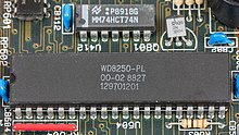
8250 UART


The 8250 UART (universal asynchronous receiver-transmitter) is an integrated circuit designed for implementing the interface for serial communications. The part was originally manufactured by the National Semiconductor Corporation. It was commonly used in PCs and related equipment such as printers or modems. The 8250 included an on-chip programmable bit rate generator, allowing use for both common and special-purpose bit rates which could be accurately derived from an arbitrary crystal oscillator reference frequency.
The chip designations carry suffix letters for later versions of the same chip series. For example, the original 8250 was soon followed by the 8250A and 8250B versions that corrected some bugs.[1][2] In particular, the original 8250 could repeat transmission of a character if the CTS line was asserted asynchronously during the first transmission attempt.[1][2]
Due to the high demand, other manufacturers soon began offering compatible chips. Western Digital offered WD8250 chip under Async Communications Interface Adapter (ACIA) and Async Communications Element (ACE) names.
The 16450(A) UART, commonly used in IBM PC/AT-series computers, improved on the 8250 by permitting higher serial line speeds.
With the introduction of multitasking operating systems on PC hardware, such as OS/2, Windows NT or various flavours of UNIX, the short time available to serve character-by-character interrupt requests became a problem, therefore the IBM PS/2 serial ports introduced the 16550(A) UARTs that had a built-in 16 byte FIFO or buffer memory to collect incoming characters.
Later models added larger memories, supported higher speeds, combined multiple ports on one chip and finally became part of the now-common Super I/O circuits combining most input/output logic on a PC motherboard.
Blocks
[edit]The line interface consists of: SOUT, SIN, /RTS, /DTR, DSR, /DCD, /CTS, /RI[3]
Clock interface: XIN, XOUT, /BAUDOUT, RCLK[3]
Computer interface: D0..D7, /RD, /WR, INTRPT, MR, A0, A1, A2, ADS, WR, RD, /CS2, CS1, CS0[3]
The interrupt line will (when the IER bit has enabled it) be triggered to go high when one of the following events occur: Receiver line status, Received data available, Transmitter holding register empty, and MODEM status. The interrupt signal is reset to low level upon the appropriate interrupt service or a reset operation (via MR).[3]
History
[edit]The 8250 UART was used in several 8-bit computers at least since 1978. IBM used the 8250 UART in the IBM PC (1981). The 8250A and 8250B revisions were later released, and the 16450 was introduced with the IBM Personal Computer/AT (1984).
The main difference between releases was the maximum communication speed.[4]
IBM refused to use Intel 8251 in the serial port adapter because Intel chip had no internal baudrate generator, and the adapter had to be more complex and expensive. Later IBM implemented Synchronous Communication Adapter, but it was not popular.
References
[edit]- ^ a b Van Gilluwe, Frank (1997). Undocumented PC (2 ed.). Addison Wesley. ISBN 0-20147950-8.
- ^ a b Paul, Matthias R. (2002-04-06). "Re: [fd-dev] ANNOUNCE: CuteMouse 2.0 alpha 1". freedos-dev. Archived from the original on 2020-02-07. Retrieved 2020-02-07. (NB. Has various information on 8250 chip bugs.)
- ^ a b c d National Semiconductor PC16450C/NS16450, PC8250A/INS8250A Universal Asynchronous Receiver Transmitter; datasheet 1990
- ^ "Serial UART, an in-depth tutorial". /NB. Focus on 16550 primarily.)
