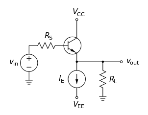
Common collector
This article includes a list of general references, but it lacks sufficient corresponding inline citations. (April 2009) |

In electronics, a common collector amplifier (also known as an emitter follower) is one of three basic single-stage bipolar junction transistor (BJT) amplifier topologies, typically used as a voltage buffer.
In this circuit the base terminal of the transistor serves as the input, the emitter is the output, and the collector is common to both (for example, it may be tied to ground reference or a power supply rail), hence its name. The analogous field-effect transistor circuit is the common drain amplifier and the analogous tube circuit is the cathode follower.
Basic circuit

The circuit can be explained by viewing the transistor as being under the control of negative feedback. From this viewpoint, a common-collector stage (Fig. 1) is an amplifier with full series negative feedback. In this configuration (Fig. 2 with β = 1), the entire output voltage Vout is placed contrary and in series with the input voltage Vin. Thus the two voltages are subtracted according to Kirchhoff's voltage law (KVL) (the subtractor from the function block diagram is implemented just by the input loop), and their difference Vdiff = Vin − Vout is applied to the base–emitter junction. The transistor continuously monitors Vdiff and adjusts its emitter voltage to equal Vin minus the mostly constant VBE by passing the collector current through the emitter resistor RE. As a result, the output voltage follows the input voltage variations from VBE up to V+; hence the name "emitter follower".
Intuitively, this behavior can be also understood by realizing that VBE is very insensitive to bias changes, so any change in base voltage is transmitted (to good approximation) directly to the emitter. It depends slightly on various disturbances (transistor tolerances, temperature variations, load resistance, a collector resistor if it is added, etc.), since the transistor reacts to these disturbances and restores the equilibrium. It never saturates even if the input voltage reaches the positive rail.
The common-collector circuit can be shown mathematically to have a voltage gain of almost unity:

A small voltage change on the input terminal will be replicated at the output (depending slightly on the transistor's gain and the value of the load resistance; see gain formula below). This circuit is useful because it has a large input impedance
so it will not load down the previous circuit, and a small output impedance
so it can drive low-resistance loads.
Typically, the emitter resistor is significantly larger and can be removed from the equation:
Applications

The low output impedance allows a source with a large output impedance to drive a small load impedance; it functions as a voltage buffer. In other words, the circuit has current gain (which depends largely on the hFE of the transistor) instead of voltage gain, because of its characteristics it is preferred in many electronic devices. A small change to the input current results in much larger change in the output current supplied to the output load.
One aspect of buffer action is transformation of impedances. For example, the Thévenin resistance of a combination of a voltage follower driven by a voltage source with high Thévenin resistance is reduced to only the output resistance of the voltage follower (a small resistance). That resistance reduction makes the combination a more ideal voltage source. Conversely, a voltage follower inserted between a small load resistance and a driving stage presents a large load to the driving stage—an advantage in coupling a voltage signal to a small load.
This configuration is commonly used in the output stages of class-B and class-AB amplifiers. The base circuit is modified to operate the transistor in class-B or AB mode. In class-A mode, sometimes an active current source is used instead of RE (Fig. 4) to improve linearity and/or efficiency.[1]
Characteristics
At low frequencies and using a simplified hybrid-pi model, the following small-signal characteristics can be derived. (Parameter and the parallel lines indicate components in parallel.)
| Definition | Expression | Approximate expression | Conditions | |
|---|---|---|---|---|
| Current gain | ||||
| Voltage gain | ||||
| Input resistance | ||||
| Output resistance |
Where is the Thévenin equivalent source resistance.
Derivations


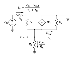
Figure 5 shows a low-frequency hybrid-pi model for the circuit of Figure 3. Using Ohm's law, various currents have been determined, and these results are shown on the diagram. Applying Kirchhoff's current law at the emitter one finds:
Define the following resistance values:
Then collecting terms the voltage gain is found:
From this result, the gain approaches unity (as expected for a buffer amplifier) if the resistance ratio in the denominator is small. This ratio decreases with larger values of current gain β and with larger values of . The input resistance is found as
The transistor output resistance ordinarily is large compared to the load , and therefore dominates . From this result, the input resistance of the amplifier is much larger than the output load resistance for large current gain . That is, placing the amplifier between the load and the source presents a larger (high-resistive) load to the source than direct coupling to , which results in less signal attenuation in the source impedance as a consequence of voltage division.
Figure 6 shows the small-signal circuit of Figure 5 with the input short-circuited and a test current placed at its output. The output resistance is found using this circuit as
Using Ohm's law, various currents have been found, as indicated on the diagram. Collecting the terms for the base current, the base current is found as
where is defined above. Using this value for base current, Ohm's law provides
Substituting for the base current, and collecting terms,
where || denotes a parallel connection, and is defined above. Because generally is a small resistance when the current gain is large, dominates the output impedance, which therefore also is small. A small output impedance means that the series combination of the original voltage source and the voltage follower presents a Thévenin voltage source with a lower Thévenin resistance at its output node; that is, the combination of voltage source with voltage follower makes a more ideal voltage source than the original one.
See also
- Common base
- Common emitter
- Common gate
- Common drain
- Common source
- IC power-supply pin
- Open collector
- Two-port network


![{\displaystyle {\begin{aligned}{\frac {1}{R_{\text{E}}}}&={\frac {1}{R_{\text{L}}}}+{\frac {1}{r_{\text{O}}}},\\[2pt]R&={\frac {R_{\text{S}}+r_{\pi }}{\beta +1}}.\end{aligned}}}](https://wikimedia.org/api/rest_v1/media/math/render/svg/6a20400874ed7f8a83fdbfd7e3f511af61720b96)


