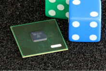
GP5 chip

The GP5 is an ASIC built to accelerate discrete belief propagation on factor graphs. It is designed to run as a co-processor with another controller (such as a CPU or an ARM core). It was developed as the culmination of DARPA's Analog Logic program [1] (although the GP5 chip itself is digital).
The GP5 has a fairly exotic architecture, resembling neither a GPU nor a DSP, and leverages massive fine-grained and coarse-grained parallelism. It is deeply pipelined. The different algorithmic tasks involved in performing belief propagation updates are performed by independent, heterogeneous compute units. The performance of the chip is governed by the structure of the factor graph being evaluated. In typical cases, the GP5 is roughly 10 times faster and 100 times more energy efficient than a single core of a modern core i7 performing a comparable task.
References
- ^ DARPA FA8750-07-C-0231
