Stacking fault

In crystallography, a stacking fault is a type of defect which characterizes the disordering of crystallographic planes. It is thus considered a planar defect.[1][2]
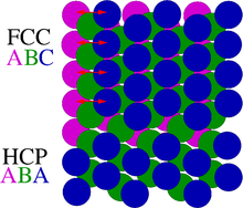
The most common example of stacking faults is found in close-packed crystal structures. Face-centered cubic (fcc) structures differ from hexagonal close packed (hcp) structures only in stacking order: both structures have close-packed atomic planes with sixfold symmetry — the atoms form equilateral triangles. When stacking one of these layers on top of another, the atoms are not directly on top of one another. The first two layers are identical for hcp and fcc, and labelled AB. If the third layer is placed so that its atoms are directly above those of the first layer, the stacking will be ABA — this is the hcp structure, and it continues ABABABAB. However, there is another possible location for the third layer, such that its atoms are not above the first layer. Instead, it is the atoms in the fourth layer that are directly above the first layer. This produces the stacking ABCABCABC, and is actually the [111] direction of a cubic crystal structure. In this context, a stacking fault is a local deviation from one of the close-packed stacking sequences to the other one. Usually, only one- two- or three-layer interruptions in the stacking sequence are referred to as stacking faults. An example for the fcc structure is the sequence ABCABABCAB.
Stacking faults carry a given formation enthalpy per unit area; this is called stacking-fault energy.
Stacking faults in semiconductors
Many compound semiconductors, e.g. those combining elements from groups III and V or from groups II and VI of the periodic table, crystallize in the fcc zincblende or hcp wurtzite crystal structures. In a semiconductor crystal, the fcc and hcp phases of a given material will usually have different band gap energies. As a consequence, when the crystal phase of a stacking fault has a lower band gap than the surrounding phase, it forms a quantum well, which in photoluminescence experiments leads to light emission at lower energies (longer wavelengths) than for the bulk crystal.[3] In the opposite case (higher band gap in the stacking fault), it constitutes an energy barrier in the band structure of the crystal that can affect the current transport in semiconductor devices.
References
- ^ Fine, Morris E. (1921). "Introduction to Chemical and Structural Defects in Crystalline Solids", in Treatise on Solid State Chemistry Volume 1, Springer.
- ^ Hirth, J. P.; Lothe, J. (1992). Theory of dislocations (2 ed.). Krieger Pub Co. ISBN 0-89464-617-6.
{{cite book}}: Unknown parameter|lastauthoramp=ignored (|name-list-style=suggested) (help) - ^ Lähnemann, J.; Jahn, U.; Brandt, O.; Flissikowski, T.; Dogan, P.; Grahn, H.T. (2014). "Luminescence associated with stacking faults in GaN". J. Phys. D: Appl. Phys. 47: 423001. arXiv:1405.1261. Bibcode:2014JPhD...47P3001L. doi:10.1088/0022-3727/47/42/423001.
