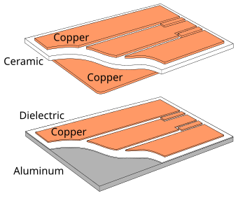
Power electronic substrate
The role of the substrate in power electronics is to provide the interconnections to form an electric circuit (like a printed circuit board), and to cool the components. Compared to materials and techniques used in lower power microelectronics, these substrates must carry higher currents and provide a higher voltage isolation (up to several thousand volts). They also must operate over a wide temperature range (up to 150 or 200 °C).
Direct bonded copper substrate

Direct bonded copper (DBC) substrates are commonly used in power modules, because of their very good thermal conductivity. They are composed of a ceramic tile (commonly alumina) with a sheet of copper bonded to one or both sides by a high-temperature oxidation process (the copper and substrate are heated to a carefully controlled temperature in an atmosphere of nitrogen containing about 30 ppm of oxygen; under these conditions, a copper-oxygen eutectic forms which bonds successfully both to copper and the oxides used as substrates). The top copper layer can be preformed prior to firing or chemically etched using printed circuit board technology to form an electrical circuit, while the bottom copper layer is usually kept plain. The substrate is attached to a heat spreader by soldering the bottom copper layer to it.
Ceramic material used in DBC include:
- Alumina (Al2O3), which is widely used because of its low cost. It is however not a really good thermal conductor (24-28 W/mK) and is brittle.[1]
- Aluminium nitride (AlN), which is more expensive, but has far better thermal performance (> 150 W/mK).
- Beryllium oxide (BeO), which has good thermal performance, but is often avoided because of its toxicity when the powder is ingested or inhaled.
One of the main advantages of the DBC substrates is their low coefficient of thermal expansion, which is close to that of silicon (compared to pure copper). This ensures good thermal cycling performances (up to 50,000 cycles).[2] The DBC substrates also have excellent electrical insulation and good heat spreading characteristics.[3]
A related technique uses a seed layer, photoimaging, and then additional copper plating to allow for fine lines (as small as 50 micrometres) and through-vias to connect front and back sides. This can be combined with polymer-based circuits to create high density substrates that eliminate the need for direct connection of power devices to heat sinks.[4]
Active metal brazed substrate
Another technology to attach thick metal layers to ceramic plates is the AMB (active metal braze) technology. With this process a metal foil is soldered to the ceramic using als[clarification needed] solder paste and high temperature (800 °C – 1000 °C). The process itself requires vacuum. Therefore, though AMB is electrically very similar to DBC, it is only suited for small production lots.
Insulated metal substrate
Insulated metal substrate (IMS) consists of a metal baseplate (aluminium is commonly used because of its low cost and density) covered by a thin layer of dielectric (usually an epoxy-based layer) and a layer of copper (35 µm to more than 200 µm thick). The FR-4-based dielectric is usually thin (about 100 μm) because it has poor thermal conductivity compared to the ceramics used in DBC substrates.
Due to its structure, the IMS is a single-sided substrate, i.e. it can only accommodate components on the copper side. In most applications, the baseplate is attached to a heatsink to provide cooling, usually using thermal grease and screws. Some IMS substrates are available with a copper baseplate for better thermal performances.
Compared to a classical printed circuit board, the IMS provides a better heat dissipation. It is one of the simplest way to provide efficient cooling to surface mount components.[5] [6]
Other substrates
- When the power devices are attached to a proper heatsink, there is no need for a thermally efficient substrate. Classical printed circuit board (PCB) material can be used (this method is typically used with through-hole technology components). This is also true for low-power applications (from some milliwatts to some watts), as the PCB can be thermally enhanced by using thermal vias or wide tracks to improve convection. An advantage of this method is that multilayer PCB allows design of complex circuits, whereas DBC and IMS are mostly single-sided technologies.[7]
- Flexible substrates can be used for low-power applications. As they are built using Kapton as a dielectric, they can withstand high temperatures and high voltages. Their intrinsic flexibility makes them resistant to thermal cycling damage.
- Ceramic substrates (thick film technology) can also be used in some applications (such as automotive) where reliability is of highest importance.[8] Compared to DCBs, thick film technology offers a higher degree of design freedom but may be less cost-efficient.
- The thermal performances of IMS, DBC and thick film substrate are evaluated in Thermal analysis of high-power modules Van Godbold, C., Sankaran, V.A. and Hudgins, J.L., IEEE Transactions on Power Electronics, Vol. 12, N° 1, Jan 1997, pages 3–11, ISSN 0885-8993 [4] (restricted access)
References
- ^ Source: Liu, Xingsheng (February 2001). "Processing and Reliability Assessment of Solder Joint Interconnection for Power Chips". Virginia Tech Dissertation [1]
- ^ Source: Curamik, manufacturer of DBC
- ^ Source: Liu, Xingsheng (February 2001). "Processing and Reliability Assessment of Solder Joint Interconnection for Power Chips". Virginia Tech Dissertation [2]
- ^ Source: Hytel Group, manufacturer of copper on ceramic substrates Archived 22 February 1999 at the Wayback Machine
- ^ Source: The Bergquist company Archived 8 February 2006 at the Wayback Machine
- ^ Source: AI Technology, Inc Archived 28 September 2007 at the Wayback Machine
- ^ Thermal Management in High-Density Power Converters , Martin März, International Conference on Industrial Technology
ICIT'03 Maribor, Slovenia, 10–12 December 2003 "Archived copy" (PDF). Archived from the original (PDF) on 13 June 2007. Retrieved 6 May 2006.
{{cite web}}: CS1 maint: archived copy as title (link) (pdf document, last accessed 6/5/06) - ^ Quick presentation of several applications and features of the thick film substrates [3]
