
Pad cratering
Pad cratering is a mechanically induced fracture in the resin between copper foil and outermost layer of fiberglass of a printed circuit board (PCB). It may be within the resin or at the resin to fiberglass interface.
The pad remains connected to the component (usually a Ball Grid Array, BGA) and leaves a "crater" on the surface of the printed circuit board.
IPC T-50, Revision H, Terms and Definitions for Interconnecting and Packaging Electronic Circuits, 96.2176 - Pad Cratering. A separation of the pad from the printed board resin/weave composite or within the composite immediately adjacent to the pad as a result of mechanical and/or thermal stress.
-
 BGA pad and solder ball exhibiting pad cratering.
 -
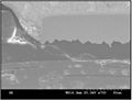 Magnified view of cross section of BGA pad and solder ball. Dielectric has cracked and the pad has started to lift, eventually creating pad cratering.
 -
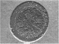 Pad crater left on printed circuit board after copper pad from a BGA connection has been pulled away.


External links
Additional information on pad cratering in printed circuit boards can be found in the following links:
- http://www.smtnet.com/Forums/index.cfm?fuseaction=view_thread&Thread_ID=13953
- http://www.pcb007.com/pages/zone.cgi?a=51651&_pf_=1
- http://knol.google.com/k/rocky-hilburn/pad-cratering-in-printed-circuit-boards/tsdgpflq7la1/1#
- http://www.ipc.org/de/ContentPage.aspx?pageid=IPC-ehrt-Best-Papers-an-der-IPC-APEX-EXPO
- http://integral-hdi.com Integral Technology
- http://integral-hdi.com/news/2010/11/next-generation-electronic-materials- Integral Technology pad cratering blog.