Through-hole technology
It has been suggested that this article be merged into Printed circuit board. (Discuss) Proposed since December 2011. |
This article includes a list of general references, but it lacks sufficient corresponding inline citations. (December 2011) |
This article needs additional citations for verification. (November 2011) |


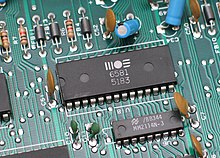
Through-hole technology, also spelled "thru-hole", refers to the mounting scheme used for electronic components that involves the use of leads on the components that are inserted into holes drilled in printed circuit boards (PCB) and soldered to pads on the opposite side either by manual assembly by hand placement or by the use of automated insertion mount machines.[1]
Through-hole technology almost completely replaced earlier electronics assembly techniques such as point-to-point construction. From the second generation of computers in the 1950s until surface-mount technology (SMT) became popular in the late 1980s, every component on a typical PCB was a through-hole component. PCBs initially had tracks printed on one side only, later both sides, then multi-layer boards were in use. Through holes became plated-through holes (PTH) in order for the components to make contact with the required layers. Plated-through holes are no longer required with SMT boards for making the component connections but are still used for making interconnections between the layers and in this role are more usually called vias.
While through-hole mounting provides strong mechanical bonds when compared to SMT techniques, the additional drilling required makes the boards more expensive to produce. They also limit the available routing area for signal traces on layers immediately below the top layer on multilayer boards since the holes must pass through all layers to the opposite side. To that end, through-hole mounting techniques are now usually reserved for bulkier components such as electrolytic capacitors or semiconductors in larger packages such as the TO220 that require the additional mounting strength, or for components such as plug connectors or electromechanical relays that require great strength in support.
Design engineers often prefer the larger through-hole to surface mount parts when prototyping because they can be used with breadboards, making them easier to handle, insert, and solder.
A rule of thumb for creating a through-hole on a PCB is to make the drill diameter 0.019” (0.48 mm) larger than the part’s lead.[citation needed] Horizontal installation of axial-leaded through-hole parts (e.g., resistor, capacitors, and diodes) is done by bending the leads 90° in the same direction, inserting part in the board, bending leads located on the back of the board in opposing directions to improve the part's mechanical strength; finally, soldering the leads such that the solder seeps through to both sides of the board. Later the assembler cuts off the excess leads.
Installation of radial-leaded parts (e.g., LEDs and electrolytic capacitors) and ICs are done in the same manner except the parts are already formed in a 90° direction.

See also
References
- ^ Electronic Packaging:Solder Mounting Technlogies in K.H. Buschow et al (ed), Encyclopedia of Materials:Science and Technolgy, Elsevier, 2001 ISBN 0-08-043152-6, pages 2708-2709
- Lesser, Roger; Alderton, Megan (January 1, 2002). "The Future of Commercial Aviation". Mobile Development and Design Magazine. Retrieved December 30, 2011.
{{cite web}}: External link in|publisher= - "Flexible production cell for led arrays. (Spotlight: electronic displays)". Canadian Electronics. March 1, 2003. Retrieved December 30, 2011. (subscription required)
- Khan, Zulki (February 1, 2010). "Component Layout in Placement Processes". Printed Circuit Design & Fab. Retrieved December 30, 2011.
{{cite web}}: External link in|publisher= - Template:Fr-icon Charpentier, Stephane (March 10, 2010). "Fabrication: Visiting a production line of [[Kingston Technology|Kingston]] memory modules". PC World (France). Retrieved December 30, 2011.
{{cite web}}: External link in|publisher=
External links
 hole sizes for through-hole parts at Wikibooks
