User:Azizkayihan/Diode
Equilibrium (zero bias)
[edit]In a p-n junction, without an external applied voltage, an equilibrium condition is reached in which a potential difference is formed across the junction. This potential difference is called built-in potential .
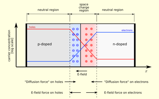
In an equilibrium PN junction, electrons near the PN interface tend to diffuse into the p region. As electrons diffuse, they leave positively charged ions (donors) on the n region. Similarly holes near the PN interface begin to diffuse in the n-type region leaving fixed ions (acceptors) with negative charge. The regions nearby the PN interfaces lose their neutrality and become charged, forming the space charge region or depletion layer (see figure A).

The electric field created by the space charge region opposes the diffusion process for both electrons and holes. There are two concurrent phenomena: the diffusion process that tends to generate more space charge, and the electric field generated by the space charge that tends to counteract the diffusion. The carrier concentration profile at equilibrium is shown in figure A with blue and red lines. Also shown are the two counterbalancing phenomena that establish equilibrium.

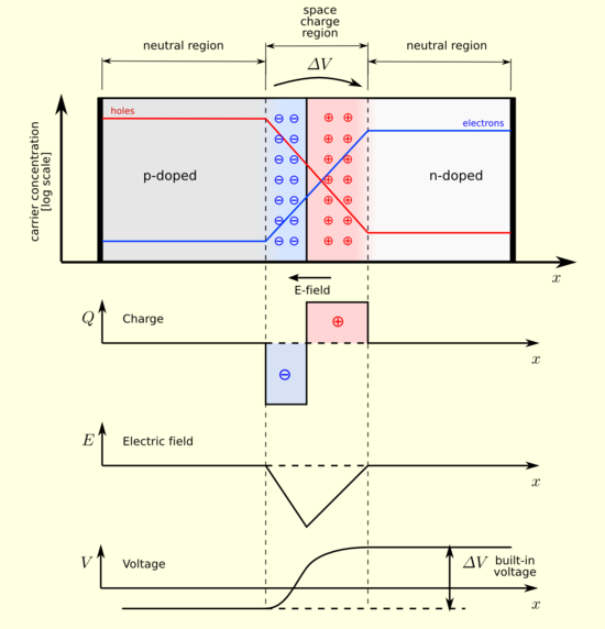
The space charge region is a zone with a net charge provided by the fixed ions (donors or acceptors) that have been left uncovered by majority carrier diffusion. When equilibrium is reached, the charge density is approximated by the displayed step function. In fact, the region is completely depleted of majority carriers (leaving a charge density equal to the net doping level), and the edge between the space charge region and the neutral region is quite sharp (see figure B). The space charge region has the same charge on both sides of the PN interfaces, thus it extends farther on the less doped side (the n side in figures A and B).
Forward-bias
[edit]Forward-bias occurs when the P-type semiconductor material is connected to the positive terminal of a battery and the N-type semiconductor material is connected to the negative terminal, as shown below.

With a battery connected this way, the holes in the P-type region and the electrons in the N-type region are pushed towards the junction. This reduces the width of the depletion zone. The positive charge applied to the P-type material repels the holes, while the negative charge applied to the N-type material repels the electrons. As electrons and holes are pushed towards the junction, the distance between them decreases. This lowers the barrier in potential. With increasing forward-bias voltage, the depletion zone eventually becomes thin enough that the zone's electric field can't counteract charge carrier motion across the p-n junction, consequently reducing electrical resistance. The electrons which cross the p-n junction into the P-type material (or holes which cross into the N-type material) will diffuse in the near-neutral region. Therefore, the amount of minority diffusion in the near-neutral zones determines the amount of current that may flow through the diode.
Only majority carriers (electrons in N-type material or holes in P-type) can flow through a semiconductor for a macroscopic length. With this in mind, consider the flow of electrons across the junction. The forward bias causes a force on the electrons pushing them from the N side toward the P side. With forward bias, the depletion region is narrow enough that electrons can cross the junction and inject into the P-type material. However, they do not continue to flow through the P-type material indefinitely, because it is energetically favorable for them to recombine with holes. The average length an electron travels through the P-type material before recombining is called the diffusion length, and it is typically on the order of microns.[1]
Although the electrons penetrate only a short distance into the P-type material, the electric current continues uninterrupted, because holes (the majority carriers) begin to flow in the opposite direction. The total current (the sum of the electron and hole currents) is constant in space, because any variation would cause charge buildup over time (this is Kirchhoff's current law). The flow of holes from the P-type region into the N-type region is exactly analogous to the flow of electrons from N to P (electrons and holes swap roles and the signs of all currents and voltages are reversed).
Therefore, the macroscopic picture of the current flow through the diode involves electrons flowing through the N-type region toward the junction, holes flowing through the P-type region in the opposite direction toward the junction, and the two species of carriers constantly recombining in the vicinity of the junction. The electrons and holes travel in opposite directions, but they also have opposite charges, so the overall current is in the same direction on both sides of the diode, as required.
The Shockley diode equation models the forward-bias operational characteristics of a p-n junction outside the avalanche (reverse-biased conducting) region.
- ^ Hook, J. R. (2001). Solid State Physics. John Wiley & Sons. ISBN 0-471-92805-4.
{{cite book}}: Unknown parameter|coauthors=ignored (|author=suggested) (help)

