Gate array: Difference between revisions
m robot Adding: it:Gate array |
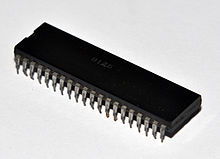
added a Picture of a ULA from my Sinclair ZX81 |
||
| Line 1: | Line 1: | ||
[[File:ZX81 ULA.jpg|thumb|Sinclair ZX81 ULA]] |
|||
A '''gate array''' or '''uncommitted logic array''' ('''ULA''') is an approach to the design and manufacture of [[application-specific integrated circuit]]s (ASICs). A gate array circuit is a prefabricated silicon chip circuit with no particular function in which [[transistor]]s, standard [[NAND]] or [[NOR]] [[logic gate]]s, and other [[active device]]s are placed at regular predefined positions and manufactured on a [[wafer (electronics)|wafer]], usually called a ''master slice''. Creation of a circuit with a specified function is accomplished by adding a final surface layer or layers of metal interconnects to the chips on the master slice late in the manufacturing process, joining these elements to allow the function of the chip to be customised as desired. This layer is analogous to the copper layer(s) of a [[printed circuit board]] (PCB). |
A '''gate array''' or '''uncommitted logic array''' ('''ULA''') is an approach to the design and manufacture of [[application-specific integrated circuit]]s (ASICs). A gate array circuit is a prefabricated silicon chip circuit with no particular function in which [[transistor]]s, standard [[NAND]] or [[NOR]] [[logic gate]]s, and other [[active device]]s are placed at regular predefined positions and manufactured on a [[wafer (electronics)|wafer]], usually called a ''master slice''. Creation of a circuit with a specified function is accomplished by adding a final surface layer or layers of metal interconnects to the chips on the master slice late in the manufacturing process, joining these elements to allow the function of the chip to be customised as desired. This layer is analogous to the copper layer(s) of a [[printed circuit board]] (PCB). |
||
Revision as of 17:52, 15 January 2011

A gate array or uncommitted logic array (ULA) is an approach to the design and manufacture of application-specific integrated circuits (ASICs). A gate array circuit is a prefabricated silicon chip circuit with no particular function in which transistors, standard NAND or NOR logic gates, and other active devices are placed at regular predefined positions and manufactured on a wafer, usually called a master slice. Creation of a circuit with a specified function is accomplished by adding a final surface layer or layers of metal interconnects to the chips on the master slice late in the manufacturing process, joining these elements to allow the function of the chip to be customised as desired. This layer is analogous to the copper layer(s) of a printed circuit board (PCB).
Gate array master slices are usually prefabricated and stockpiled in large quantities regardless of customer orders. The design and fabrication according to the individual customer specifications may be finished in a shorter time compared with standard cell or full custom design. The gate array approach reduces the mask costs since fewer custom masks need to be produced. In addition manufacturing test tooling lead time and costs are reduced since the same test fixtures may be used for all gate array products manufactured on the same die size. Gate arrays were the predecessor of the more advanced structured ASIC; unlike gate arrays, structured ASICs tend to include predefined or configurable memories and/or analog blocks. Structured ASICs are still sold by companies such as ChipX, Inc.
An application circuit must be built on a gate array that has enough gates, wiring and I/O pins. Since requirements vary, gate arrays usually come in families, with larger members having more of all resources, but correspondingly more expensive. While the designer can fairly easily count how many gates and I/Os pins are needed, the amount of routing tracks needed may vary considerably even among designs with the same amount of logic. (For example, a crossbar switch requires much more routing than a systolic array with the same gate count.) Since unused routing tracks increase the cost (and decrease the performance) of the part without providing any benefit, gate array manufacturers try to provide just enough tracks so that most designs that will fit in terms of gates and I/O pins can be routed. This is determined by estimates such as those derived from Rent's rule or by experiments with existing designs.
The main drawbacks of gate arrays are their somewhat lower density and performance compared with other approaches to ASIC design. However this style is often a viable approach for low production volumes.
Sinclair Research ported an enhanced ZX80 design to a ULA chip for the ZX81, and later used a ULA in the ZX Spectrum. A compatible chip was made in Russia as T34VG1.[1] Acorn Computers used several ULA chips in the BBC Micro, and later managed to compress almost all of that machine's logic into a single ULA for the Acorn Electron. Many other manufacturers from the time of the home computer boom period used ULAs in their machines. Ferranti in the UK pioneered ULA technology, then later abandoned this lead in semi-custom chips. The IBM PC took over much of the personal computer market, and the sales volumes made full-custom chips more economical.
Designers still wished for a way to create their own complex chips without the expense of full-custom design, and eventually this wish was granted with the arrival of the field-programmable gate array (FPGA), complex programmable logic device (CPLD), and structured ASIC. Whereas a ULA required a semiconductor wafer foundry to deposit and etch the interconnections, the FPGA and CPLD had programmable interconnections.
See also
References
- ^ Т34ВГ1 — article about the ZX Spectrum ULA compatible chip Template:Ru icon
