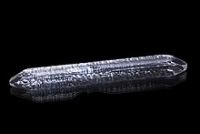
Single crystal
This article needs additional citations for verification. (February 2010) |
A single crystal or monocrystalline solid is a material in which the crystal lattice of the entire sample is continuous and unbroken to the edges of the sample, with no grain boundaries. The absence of the defects associated with grain boundaries can give monocrystals unique properties, particularly mechanical, optical and electrical, which can also be anisotropic, depending on the type of crystallographic structure. These properties, in addition to making them precious in some gems, are industrially used in technological applications, especially in optics and electronics.
Because entropic effects favor the presence of some imperfections in the microstructure of solids, such as impurities, inhomogeneous strain and crystallographic defects such as dislocations, perfect single crystals of meaningful size are exceedingly rare in nature, and are also difficult to produce in the laboratory, though they can be made under controlled conditions. On the other hand, imperfect single crystals can reach enormous sizes in nature: several mineral species such as beryl, gypsum and feldspars are known to have produced crystals several metres across.
The opposite of a single crystal is an amorphous structure where the atomic position is limited to short range order only. In between the two extremes exist polycrystalline, which is made up of a number of smaller crystals known as crystallites, and paracrystalline phases.
Uses


Semiconductor industry
Single crystal silicon is used in the fabrication of semiconductors. On the quantum scale that microprocessors operate on, the presence of grain boundaries would have a significant impact on the functionality of field effect transistors by altering local electrical properties. Therefore, microprocessor fabricators have invested heavily in facilities to produce large single crystals of silicon.
Optics
This section needs expansion. You can help by adding to it. (April 2009) |
- Monocrystals of sapphire and other materials are used for lasers and nonlinear optics.
- Monocrystals of fluorite are sometimes used in the objective lenses of apochromatic refracting telescopes.[citation needed]
Materials engineering
Another application of single crystal solids is in materials science in the production of high strength materials with low thermal creep, such as turbine blades.[1][2] Here, the absence of grain boundaries actually gives a decrease in yield strength, but more importantly decreases the amount of creep which is critical for high temperature, close tolerance part applications.
Electrical conductors
Single crystal copper has better conductivity than polycrystalline copper.[3] As of 2009, no single crystal copper is manufactured on a large scale industrially, but methods of producing very large individual crystal sizes for copper conductors are exploited for high performance electrical applications. These can be considered meta-single crystals with only a few crystals per metre of length.
In research
Single crystals are essential in research especially condensed-matter physics, materials science, surface science etc. The detailed study of the crystal structure of a material by techniques such as Bragg diffraction and helium atom scattering is much easier with monocrystals. Only in single crystals it is possible to study directional dependence of various properties. Furthermore, techniques such as scanning tunneling microscopy are only possible on surfaces of single crystals. In superconductivity there have been cases of materials where superconductivity is only seen in single crystalline specimen. They may be grown for this purpose, even when the material is otherwise only needed in polycrystalline form.
Manufacture
In the case of silicon and metal single crystal fabrication the techniques used involve highly controlled and therefore relatively slow crystallization.
Specific techniques to produce large single crystals (aka boules) include the Czochralski process and the Bridgman technique. Other less exotic methods of crystallization may be used, depending on the physical properties of the substance, including hydrothermal synthesis, sublimation, or simply solvent-based crystallization.
A different technology to create single crystalline materials is called epitaxy. As of 2009, this process is used to deposit very thin (micrometre to nanometer scale) layers of the same or different materials on the surface of an existing single crystal. Applications of this technique lie in the areas of semiconductor production, with potential uses in other nanotechnological fields and catalysis.
See also
- Engineering aspects of crystallisation
- Fractional crystallization (chemistry)
- Laser Heated Pedestal Growth
- Micro-Pulling-Down
- Recrystallization (metallurgy)
- Seed crystal
References
- ^ Spittle, Peter. "Gas turbine technology" Rolls-Royce plc, 2003. Retrieved: 21 July 2012.
- ^ Crown jewels - These crystals are the gems of turbine efficiency Article on single crystal turbine blades memagazine.com
- ^ Cho, Yong Chan (March 22, 2010). "Copper Better than Silver: Electrical Resistivity of the Grain-Free Single-Crystal Copper Wire". Crystal Growth & Design. 10: 2780–2784. doi:10.1021/cg1003808. Retrieved 1 June 2011.
{{cite journal}}: Unknown parameter|coauthors=ignored (|author=suggested) (help)

