Thin-film transistor

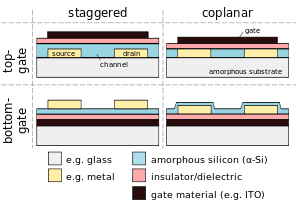
A thin-film transistor (TFT) is a special kind of field-effect transistor made by depositing thin films of an active semiconductor layer as well as the dielectric layer and metallic contacts over a supporting (but non-conducting) substrate. A common substrate is glass, because the primary application of TFTs is in liquid-crystal displays. This differs from the conventional transistor, where the semiconductor material typically is the substrate, such as a silicon wafer.
Manufacture
TFTs can be made using a wide variety of semiconductor materials. A common material is silicon. The characteristics of a silicon-based TFT depend on the silicon's crystalline state; that is, the semiconductor layer can be either amorphous silicon,[1] microcrystalline silicon,[1] or it can be annealed into polysilicon.
Other materials which have been used as semiconductors in TFTs include compound semiconductors such as cadmium selenide,[2][3] or metal oxides such as zinc oxide.[4] TFTs have also been made using organic materials, referred to as organic field-effect transistors or OTFTs.
By using transparent semiconductors and transparent electrodes, such as indium tin oxide (ITO), some TFT devices can be made completely transparent. Such transparent TFTs (TTFTs) can be used for construction of video display panels.
Because conventional substrates cannot withstand high annealing temperatures, the deposition process must be completed under relatively low temperatures. Chemical vapor deposition and physical vapor deposition (usually sputtering) are applied. The first solution-processed TTFTs, based on zinc oxide, were reported in 2003 by researchers at Oregon State University.[4] The Portuguese laboratory CENIMAT at the Universidade Nova de Lisboa has produced the world’s first completely transparent TFT at room temperature.[citation needed] CENIMAT also developed the first paper transistor,[citation needed] which may lead to applications such as magazines and journal pages with moving images.
Applications
The best known application of thin-film transistors is in TFT LCDs, an implementation of LCD technology. Transistors are embedded within the panel itself, reducing crosstalk between pixels and improving image stability.
As of 2008[update], many color LCD TVs and monitors use this technology. TFT panels are frequently used in digital radiography applications in general radiography. A TFT is used in both direct and indirect capture[jargon] as a base for the image receptor in medical radiography.
AMOLED (active-matrix organic light-emitting diode) screens also contain a TFT layer.
The most beneficial aspect[neutrality is disputed] of TFT technology is its use of a separate transistor for each pixel on the display. Because each transistor is small, the amount of charge needed to control it is also small. This allows for very fast re-drawing of the display.
Structure of a TFT-display matrix
This picture does not include the actual light-source (usually cold-cathode fluorescent lamps or white LEDs), just the TFT-display matrix.
References
- ^ a b Kanicki, Jerzy (1992). Amorphous & Microcystalline Semiconductor Devices Volume II: Materials and Device Physics. Artech House, Inc. ISBN 0-89006-379-6.
- ^ Brody, T. Peter (November 1984). "The Thin Film Transistor - A Late Flowering Bloom". IEEE Transactions on Electron Devices. 31 (11): 1614–1628. doi:10.1109/T-ED.1984.21762.
- ^ Brody, T. Peter (1996). "The birth and early childhood of active matrix - a personal memoir". Journal of the SID. 4/3: 113–127.
- ^ a b Wager, John. OSU Engineers Create World's First Transparent Transistor. College of Engineering, Oregon State University, Corvallis, OR: OSU News & Communication, 2003. 29 July 2007.

