Insulated-gate bipolar transistor: Difference between revisions
| Line 50: | Line 50: | ||
==Manufacturers== |
==Manufacturers== |
||
*[http://www.infineon.com INFINEON Technologies] |
|||
*[http://www.semikron.com SEMIKRON International GmbH] |
*[http://www.semikron.com SEMIKRON International GmbH] |
||
*[http://www.ABB.com/semiconductors ABB Switzerland Ltd Semiconductors] |
*[http://www.ABB.com/semiconductors ABB Switzerland Ltd Semiconductors] |
||
Revision as of 04:26, 3 September 2007


The Insulated Gate Bipolar Transistor is a three-terminal Power semiconductor device that combines the simple gate drive characteristics of the MOSFETs with the high current and low saturation voltage capability of bipolar transistors by combining an isolated gate FET for the control input, and a bipolar power transistor as a switch, in a single device. The IGBT is used in medium to high power applications such as Switched-mode power supply, traction motor control and induction heating. Large IGBT modules typically consist of many devices in parallel and can have very high current handling capabilities in the order of hundreds of amps with blocking voltages of 6,000 volts.
The IGBT is a fairly recent invention. The "first-generation" devices of the 1980s and early 1990s were relatively slow in switching, and prone to failure through such modes as latchup and secondary breakdown. Second-generation devices were much improved, and the current third-generation ones are even better, with speed rivaling MOSFETs, and excellent ruggedness and tolerance of overloads.
The extremely high pulse ratings of second- and third-generation devices also make them useful for generating large power pulses in areas like particle and plasma physics, where they are starting to supersede older devices like thyratrons and triggered spark gaps.
Their high pulse ratings, and low prices on the surplus market, also make them attractive to the high-voltage hobbyist for generating large amounts of high-frequency power to drive experiments like Tesla coils.
Availability of affordable, reliable IGBTs is a key enabler for electric vehicles and hybrid cars. Toyota's second generation hybrid Prius has a 50 kW IGBT inverter controlling two AC motor/generators connected to the DC battery pack.
In addition, for about 20 years Toshiba has applied IGBTs as audio amplifiers.[citation needed]
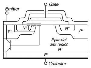
Device Structure
An IGBT cell is constructed very similar to a N-channel vertical construction Power MOSFET with a P+ region added between the drain contact and the N- drift region.

This additional P+ region creates a cascade connection of a PNP Bipolar junction transistor with the N-channel Power MOSFET. This connection results in a significantly lower forward voltage drop compared to a conventional MOSFET in higher blocking voltage rated devices. As the blocking voltage rating of both MOSFET and IGBT devices increases, the depth of the N- drift region must increase and the doping must decrease, resulting in roughly square relationship increase in forward conduction loss compared to blocking voltage capability of the device. By injecting minority carriers (holes) from the collector P+ region into the N- drift region during forward conduction, the resistance of the N- drift region is considerably reduced. This resultant reduction in on-state forward voltage comes with several penalties:
- The additional PN junction blocks reverse current flow. This means that IGBT do not reverse conduct, unlike a MOSFET. In bridge circuits where reverse current must be carried, an additional reverse diode must be added to the circuit that would not be required if a MOSFET was used. The penalty isn't as severe as first assumed though, because at the higher voltages where IGBT usage dominates, discrete diodes are of significantly higher performance than the body diode of a MOSFET. The reverse rating of the N- drift region to collector P+ diode is usually only of 10's of volts, so if the circuit application applies a reverse voltage to the IGBT, an additional series diode must be used.
- The minority carriers injected into the N- drift region take time to enter and exit or recombine at turn on and turn off. This results in longer switching time and hence higher switching loss compared to a power MOSFET.
- The additional PN junction adds a diode like voltage drop to the device. At lower blocking voltage ratings, this additional drop means that a IGBT would have a higher on state voltage drop. As the voltage rating of the device increases, the advantage of the reduction N- drift region resistance overcomes the additional diode drop and the overall on-state voltage drop is lower. This crossover is around 400V blocking rating. IGBT are rarely used where the blocking rating required is below 600V.
IGBT Models
SPICE implements Macromodels, that is models not physically based on the IGBT, but instead based on the physics models of an ensemble of components such as FETs and BJTs in a darlington configuration.
The most prominent physics based model is the Hefner model created by Allen Hefner now employeed with the NIST. Its a fairly complicated model that has shown very good results. He wrote a paper in 1988 describing this model, and extended this to a thermo-elctrical model and implemented in SABER in the years to come.
External links
See also
Manufacturers
- INFINEON Technologies
- SEMIKRON International GmbH
- ABB Switzerland Ltd Semiconductors
- IXYS Corporation
- Power-io IGBT based solid state relay
- Dynex Semiconductor Ltd.
