
Die (integrated circuit): Difference between revisions
Ashkananisi7 (talk | contribs) I changed a low quality image with my own high quality image |
Ashkananisi7 (talk | contribs) Add more images to this article |
||
| Line 2: | Line 2: | ||
[[File:LM2576T Damaged die.jpg|alt=Die of LM2576T monolithic integrated circuits step−down switching regulator (buck converter) which contains 162 active transistors (based on datasheet). The Biggest part of die on the left side is Built-in 3 Ampere power transistor and the damaged and fried part of die is clearly visible as a small black in power transistor section.|thumb|LM2576T monolithic integrated circuits die]] |
[[File:LM2576T Damaged die.jpg|alt=Die of LM2576T monolithic integrated circuits step−down switching regulator (buck converter) which contains 162 active transistors (based on datasheet). The Biggest part of die on the left side is Built-in 3 Ampere power transistor and the damaged and fried part of die is clearly visible as a small black in power transistor section.|thumb|LM2576T monolithic integrated circuits die]] |
||
A '''die''', in the context of [[integrated circuit]]s, is a small block of [[semiconducting]] material on which a given functional circuit is [[Semiconductor fabrication|fabricated]]. Typically, integrated circuits are produced in large batches on a single [[wafer (electronics)|wafer]] of electronic-grade [[Monocrystalline silicon|silicon]] (EGS) or other semiconductor (such as [[Gallium arsenide|GaAs]]) through processes such as [[photolithography]]. The wafer is cut ([[wafer dicing|diced]]) into many pieces, each containing one copy of the circuit. Each of these pieces is called a die. |
A '''die''', in the context of [[integrated circuit]]s, is a small block of [[semiconducting]] material on which a given functional circuit is [[Semiconductor fabrication|fabricated]]. Typically, integrated circuits are produced in large batches on a single [[wafer (electronics)|wafer]] of electronic-grade [[Monocrystalline silicon|silicon]] (EGS) or other semiconductor (such as [[Gallium arsenide|GaAs]]) through processes such as [[photolithography]]. The wafer is cut ([[wafer dicing|diced]]) into many pieces, each containing one copy of the circuit. Each of these pieces is called a die. |
||
[[File:1 watt red power led.jpg|thumb|1 watt red power led die.]] |
|||
There are three commonly used plural forms: ''dice'', ''dies,'' and ''die''.<ref>{{cite book | title = Digital Integrated Circuits | author = John E. Ayers | publisher = CRC Press | year = 2004 | isbn = 0-8493-1951-X | url = https://books.google.com/books?id=QHtalNXHKbsC&q=die+dice+dies+plural+wafer&pg=PA31 | url-status = live | archive-url = https://web.archive.org/web/20170131014137/https://books.google.com/books?id=QHtalNXHKbsC&pg=PA31&dq=die+dice+dies+plural+wafer&lr=&as_brr=3&ei=hakESZTiJJGssgO9yNGqBA | archive-date = 2017-01-31 }}</ref><ref>{{cite book | title = Encyclopedia of Physical Science and Technology | author = Robert Allen Meyers | publisher = Academic Press | year = 2000 | isbn = 0-12-226930-6 | url = https://books.google.com/books?id=C4gyAAAAMAAJ&q=chips+dies+plural+wafer }}</ref> To simplify handling and integration onto a [[printed circuit board]], most dies are [[integrated circuit packaging|packaged]] in [[list of integrated circuit packaging types|various forms]]. |
There are three commonly used plural forms: ''dice'', ''dies,'' and ''die''.<ref>{{cite book | title = Digital Integrated Circuits | author = John E. Ayers | publisher = CRC Press | year = 2004 | isbn = 0-8493-1951-X | url = https://books.google.com/books?id=QHtalNXHKbsC&q=die+dice+dies+plural+wafer&pg=PA31 | url-status = live | archive-url = https://web.archive.org/web/20170131014137/https://books.google.com/books?id=QHtalNXHKbsC&pg=PA31&dq=die+dice+dies+plural+wafer&lr=&as_brr=3&ei=hakESZTiJJGssgO9yNGqBA | archive-date = 2017-01-31 }}</ref><ref>{{cite book | title = Encyclopedia of Physical Science and Technology | author = Robert Allen Meyers | publisher = Academic Press | year = 2000 | isbn = 0-12-226930-6 | url = https://books.google.com/books?id=C4gyAAAAMAAJ&q=chips+dies+plural+wafer }}</ref> To simplify handling and integration onto a [[printed circuit board]], most dies are [[integrated circuit packaging|packaged]] in [[list of integrated circuit packaging types|various forms]]. |
||
| Line 9: | Line 9: | ||
Most dies are composed of silicon and used for integrated circuits. The process begins with the production of monocrystalline silicon ingots. These ingots are then sliced into disks with a diameter of up to 300 mm.<ref> [https://www.youtube.com/watch?v=Q5paWn7bFg4 From Sand to Silicon “Making of a Chip” | Intel]. (YouTube video, streamed on Nov 6, 2009) </ref><ref> |
Most dies are composed of silicon and used for integrated circuits. The process begins with the production of monocrystalline silicon ingots. These ingots are then sliced into disks with a diameter of up to 300 mm.<ref> [https://www.youtube.com/watch?v=Q5paWn7bFg4 From Sand to Silicon “Making of a Chip” | Intel]. (YouTube video, streamed on Nov 6, 2009) </ref><ref> |
||
[https://web.archive.org/web/20150816080137/http://download.intel.com/pressroom/kits/chipmaking/Making_of_a_Chip.pdf From Sand to Silicon “Making of a Chip” Illustrations]. (n.d.) </ref> |
[https://web.archive.org/web/20150816080137/http://download.intel.com/pressroom/kits/chipmaking/Making_of_a_Chip.pdf From Sand to Silicon “Making of a Chip” Illustrations]. (n.d.) </ref> |
||
[[File:Typical NPN Transistor.jpg|thumb|'''Typical NPN Transistor. size of die is roughly 1mm x 1mm .''']] |
|||
These wafers are then polished to a mirror finish before going through [[photolithography]]. In many steps the transistors are manufactured and connected with metal interconnect layers. These prepared wafers then go through [[wafer testing]] to test their functionality. The wafers are then sliced and sorted to filter out the faulty dies. Functional dies are then [[Integrated circuit packaging|packaged]] and the completed integrated circuit is ready to be shipped. |
These wafers are then polished to a mirror finish before going through [[photolithography]]. In many steps the transistors are manufactured and connected with metal interconnect layers. These prepared wafers then go through [[wafer testing]] to test their functionality. The wafers are then sliced and sorted to filter out the faulty dies. Functional dies are then [[Integrated circuit packaging|packaged]] and the completed integrated circuit is ready to be shipped. |
||
| Line 24: | Line 24: | ||
File:Diopsis.jpg|A [[Very-large-scale integration|VLSI]] integrated-circuit die |
File:Diopsis.jpg|A [[Very-large-scale integration|VLSI]] integrated-circuit die |
||
File:Pentiumpro moshen.jpg|Two dies bonded onto one [[chip carrier]] |
File:Pentiumpro moshen.jpg|Two dies bonded onto one [[chip carrier]] |
||
File:Burr- |
File:Burr-Brown OPA103.jpg|A monolithic IC operational amplifier |
||
File:ICM7107.jpg|3 1/2 Digit Single Chip A/D Converter |
File:ICM7107.jpg|3 1/2 Digit Single Chip A/D Converter |
||
File: |
File:SN7400 1965.jpg|SN7400 Quad NAND gate in flat pack package. 1965. |
||
File:CD-ROM Drive head die.jpg|CD-ROM Drive head die |
|||
</gallery> |
</gallery> |
||
Revision as of 00:54, 25 January 2024

A die, in the context of integrated circuits, is a small block of semiconducting material on which a given functional circuit is fabricated. Typically, integrated circuits are produced in large batches on a single wafer of electronic-grade silicon (EGS) or other semiconductor (such as GaAs) through processes such as photolithography. The wafer is cut (diced) into many pieces, each containing one copy of the circuit. Each of these pieces is called a die.

There are three commonly used plural forms: dice, dies, and die.[1][2] To simplify handling and integration onto a printed circuit board, most dies are packaged in various forms.
Manufacturing process
Most dies are composed of silicon and used for integrated circuits. The process begins with the production of monocrystalline silicon ingots. These ingots are then sliced into disks with a diameter of up to 300 mm.[3][4]
These wafers are then polished to a mirror finish before going through photolithography. In many steps the transistors are manufactured and connected with metal interconnect layers. These prepared wafers then go through wafer testing to test their functionality. The wafers are then sliced and sorted to filter out the faulty dies. Functional dies are then packaged and the completed integrated circuit is ready to be shipped.
Uses
A die can host many types of circuits. One common use case of an integrated circuit die is in the form of a Central Processing Unit (CPU). Through advances in modern technology, the size of the transistor within the die has shrunk exponentially, following Moore's Law. Other uses for dies can range from LED lighting to power semiconductor devices.
Images
-
 Single NPN bipolar junction transistor die
 -
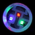 Close-up of an RGB light-emitting diode, showing the three individual dies
 -
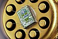
 A small-scale integrated circuit die, with bond wires attached
 -
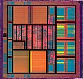 A VLSI integrated-circuit die
 -
 Two dies bonded onto one chip carrier
 -
 A monolithic IC operational amplifier
 -
 3 1/2 Digit Single Chip A/D Converter
 -
 SN7400 Quad NAND gate in flat pack package. 1965.
 -
 CD-ROM Drive head die


See also
References
- ^ John E. Ayers (2004). Digital Integrated Circuits. CRC Press. ISBN 0-8493-1951-X. Archived from the original on 2017-01-31.
- ^ Robert Allen Meyers (2000). Encyclopedia of Physical Science and Technology. Academic Press. ISBN 0-12-226930-6.
- ^ From Sand to Silicon “Making of a Chip” | Intel. (YouTube video, streamed on Nov 6, 2009)
- ^ From Sand to Silicon “Making of a Chip” Illustrations. (n.d.)
External links
- Wedge Bonding Process on YouTube – animation
| Authority control databases: National |
|---|