
CrysTBox
 | |
Screenshot  | |
| Developer(s) | Miloslav Klinger |
|---|---|
| Initial release | 9 December 2014 |
| Written in | MATLAB |
| Operating system | Microsoft Windows |
| Available in | English |
| Type | Scientific |
| License | Free for non-commercial use |
| Website | crystbox.fzu.cz |
CrysTBox (Crystallographic Tool Box) is a set of computer tools for crystallographic visualization and analysis of transmission electron microscope images. It became popular among electron crystallographers thanks to the use of artificial intelligence and computer vision which makes routine diffraction analysis faster, easier and more accurate than manual evaluation. The high level of automation together with sub-pixel precision[1] and interactive visualization makes the quantitative crystallographic analysis accessible even for non-crystallographers. Therefore, CrysTBox is not specifically limited to material science but is also suitable for education and interdisciplinary research.
CrysTBox is being developed in the Laboratory of electron microscopy at the Institute of Physics of the Czech Academy of Sciences. For academic purposes, it is available for free. By the end of 2021, it has been used in more than 80 countries.[2]
Tool box
The tool box consists of four analytical tools for automated processing of electron microscope images and two visualization tools.
Availability
CrysTBox is freely available on demand for non-commercial use by non-commercial subjects. Commercial use is not allowed due to the license of MATLAB used for CrysTBox compilation.
Input data
The primary input is the structure of sample material. In CrysTBox, materials can be specified using Cyrstallographic information file or by creating a simple text file. A basic set of several hundred materials is included in the CrysTBox package. Other materials can be obtained via databases such as Crystallography Open Database or Inorganic Crystal Structure Database.
Analytical tools also require the image to be processed (electron diffraction, high-resolution image etc.). Supported image formats include common formats such as PNG, JPEG, BMP or TIFF as well as specialized ones – DM2 a DM3. Example images are included allowing the user to get familiar with individual tools.
Connectivity
The tools can be used separately as well as chained together – for instance the sample orientation can be determined using diffractGUI and consequently visualized in cellViewer as an appropriately oriented unit cell accompanied by a simulated diffraction pattern. The tools can be also launched by other software through instructions passed via a special text file. This allows CrysTBox to be interconnected with other software such as DigitalMicrograph 1 and 2.
Limitations and disadvantages
CrysTBox is compiled to a stand-alone installers using MATLAB Compiler. Therefore, 1-2 GB of MATLAB libraries are installed together with the toolbox.
The diffraction simulation used in cellViewer is based on kinematic diffraction theory. This allows for a real-time response to user interaction, but it does not cover advanced diffraction features like double diffraction covered by dynamical diffraction theory.
The analytical tools provide correction for scale calibration imperfections, but does not provide adjustment for image distortions such as elliptical distortion. If high-accuracy measurement is needed or if the distortion exceeds standard levels, appropriate tools[3] should be applied prior to the analysis.
Visualization tools
In order to visualize functional relations and provide better understanding of experimental data, the graphical representations emphasize user interactivity and functional interconnection.
cellViewer
CellViewer allows to visualize the sample material in four modes widely used in material research:
- 3D model of atomic structure (direct space),
- simulated diffraction pattern (reciprocal space),
- stereographic projection (projection of 3D space of crystallographic planes and directions to 2D),
- inverse pole figure (defined part of stereographic projection).
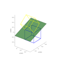
Graphical user interface provides user with two interactive views side by side. These views can display arbitrary combination of the four aforementioned visualization modes allowing to perceive their mutual relations. For instance, rotation of the atomic structure in direct space leads (if set so) to an instant update of the simulated diffraction pattern. If any diffraction spot is selected, corresponding crystallographic planes are shown in the unit cell etc. Such interconnections are implemented for each pair of the four available visualization modes. The electronic visualization allows to simplify understanding of widely used, yet less intuitive representations such as the inverse pole figure. For instance by drawing the coloured triangle of the inverse pole figure into the stereographic projection or to the more intuitive 3D atomic structure.
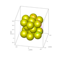
- Examples of various usage of visualization modes with magnesium as sample material
-
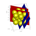 3D atomic structure with selected planes
 -
 Diffraction pattern with selected reflections (planes)
 -
 3D atomic structure with inverse pole figure
 -
 Stereographic projection with inverse pole figure
 -
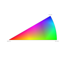 Inverse pole figure


ifaceViewer

The ifaceViewer allows for visualization of two misoriented materials and their interface such as crystal twins or grain boundaries. The user interface provides three views: two smaller views, each depicting one unit cell of selected material and orientation, and a larger view depicting an appropriate interface of the two structures. The interface can be visualized in four modes:
- 3D model of both unit cells,
- wire model of both unit cells,
- cross section of the interface,
- bulk representation (up to several hundred atoms).
All three views in the user interface are functionally interconnected. If the content of one view is rotated by the user, the other views follow. If a crystallographic plane or direction is selected in one view, it is shown in other views and corresponding crystallographic indices are stated. The tool also allows to highlight coincident site lattice or calculate the list of planes and directions which are parallel or nearly parallel in the two misoriented materials.
- Interface of two aluminum lattices in Σ5 misorientation shown in four available visualization modes of CrysTBox IfaceViewer
-
 3D model of both unit cells
 -
 Wire model of both unit cells
 -
 Interface cross section
 -
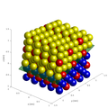 Bulk representation


Analytical tools
Since the analytical tools employ algorithms of artificial intelligence and computer vision, they are designed to automatically process transmission electron microscope images returning indexed patterns, measured interplanar distances, angles, sample thickness etc. Despite the high level of automation, the user is able to control the whole process and perform individual steps manually if needed.
diffractGUI

DiffractGUI allows to determine crystal orientation from a diffraction pattern of high-resolution image, to identify individual diffraction spots and to measure interplanar angles and distances in picometric precision.[4] The input image may depict:
- selected area diffraction,
- high-resolution image,
- nanodiffraction pattern or
- convergent beam electron diffraction.
The input image is processed in the following steps:
- Preprocessing with accordance to the settings and image nature (resolution and noise reduction, Fourier transform for direct space images etc.).
- Detection of diffraction reflections at various scales (difference of Gaussians typically used for spot detection, Hough transform for CBED disk detection).
- The strongest detections are selected across the scale space.
- A regular lattice is fit to the set of the strongest detections using RANSAC algorithm.
- Lengths and angles of the lattice basis vectors are measured.
- Crystal lattice orientation is determined and diffraction reflections are identified using theoretical parameters of the sample material.
Compared to human evaluation, diffractGUI considers tens of diffraction spots at once and, therefore, can localize the pattern with sub-pixel precision.
- Individual steps of automated procedure illustrated on diffraction pattern of titanium
-
 Input image
 -
 30 strongest reflections detected
 -
 Regular lattice
 -
 Lattice basis and parameters measured
 -
![Reflections identified for zone axis [0 -1 1]](//upload.wikimedia.org/wikipedia/commons/thumb/b/b2/DiffractGUI_reflections.png/120px-DiffractGUI_reflections.png) Reflections identified for zone axis [0 -1 1]
Reflections identified for zone axis [0 -1 1]


![Reflections identified for zone axis [0 -1 1]](/wiki/File:DiffractGUI_reflections.png)
ringGUI

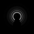
RingGUI allows for an automated processing of ring diffraction images of polycrystalline or powder samples. It can be used to identify the diffraction rings, quantify the interplanar distances and thus characterize or identify the sample material. With known material, it can assist in microscope calibration. The input image is processed as follows:
- beam-stopper detection,
- localization of the ring center,
- quantification of the diffraction profile and estimation of its background intensity,
- identification of the rings in the image (peaks in the profile).
The results can be further processed and visualized in two interactive, functionally interconnected graphical elements:
- Interactive diffraction image – allows the user to improve readability of the diffraction image by removing the beam-stopper, subtracting the background, revealing faint or spotty rings or by crystallographic identification of the depicted rings.
- Diffraction profile – circular average of the image intensities depicts the peaks corresponding to the rings and their match with theoretical values known for given sample material.
Both, the diffraction image as well as diffraction profile can be used to select diffraction rings with a mouse click. The corresponding ring is then highlighted in both graphical representations and details are listed.
- Examples of patrtial and final results presented via interactive diffraction image of MgO
-
 Input image
 -
 Beam-stopper detected
 -
 Ring centre localized
 -
 Background removed
 -
 Beam-stopper removed
 -
 Background and beam-stopper removed with faint rings revealed
 -
 Rings identified
 -
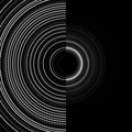 Comparison of experimental and theoretical rings


twoBeamGUI

Sample thickness can be estimated using twoBeamGUI from a convergent beam electron diffraction pattern (CBED) in two beam approximation. The procedure is based on an automated extraction of the intensity profile across the diffracted disk in the following steps:
- diffraction disk radius is determined using multi-scale Hough transform,
- the transmitted and diffracted disks are localized and the reflection is indexed,
- the disks are horizontally aligned, cropped out and profiles are measured across the disks,
- the profile across the diffracted disk is matched with a series of profiles simulated for given material, reflection and specified thickness range.
Once the procedure is completed, the measured profile and the most similar simulated profile are displayed with the diffracted disk on the background. This allows the user to verify correctness of the automated estimate and easily check the similarity of other intensity profiles within the specified thickness range.
- Individual steps of automated thickness estimation of titanium sample
-
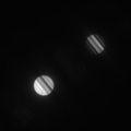 Input image
 -
 Disks detected
 -
 Disks aligned with profiles measured
 -
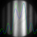 Comparison of measured (blue) and simulated (green) profile for thickness of 139 nm


gpaGUI

The tool called gpaGUI provides an interactive interface for Geometric Phase Analysis, which allows to generate 2D maps of various crystallographic quantities using high-resolution images. The high-resolution image needs to be Fourier-transformed into frequential representation. Mathematically, the frequential image is a complex matrix with the size equal to the original image. Crystallographically, it can be seen as an artificial diffraction pattern of the original image depicting intensity peaks corresponding to the crystallographic planes present in the original image. The frequential representation can be transformed back to the original image using inverse Fourier transform. If the frequential image is filtered so that only the information from a region close to a particular diffraction spot is used (the rest is set to zero), a filtered direct image obtained by inverse Fourier transform then depicts only the planes corresponding to the selected diffraction spot. Moreover, due to its complex nature, the frequential image can be used to calculate amplitude and phase. Together with a vector of one crystallographic plane depicted in the image, they can be used to generate a 2D map d-spacing.[5] If two vectors of non-parallel planes are known, the method can be used to generate maps of strain and displacement.[6]
Graphical user interface of gpaGUI is vertically divided into two halves, each of which contains:
- Diffractogram preview allowing to select one diffraction spot corresponding to a crystallographic plane.
- Visualization of a selected quantity (input image, filtered image or one of the maps mentioned above) allowing to select point of interest or region of interest for further analysis.
- Results of detailed analysis of point or region of interest. The point analysis allows the user to select any pixel of the visualized map to see exact values of the particular pixel and its closest neighbourhood. If analysis of broader area is needed, a polygonal region can be outlined in the map allowing to enumerate its statistical details: mean, standard deviation, median, minimum, maximum and total area of the polygon.
Since each half of the interface allows to specify one crystallographic plane, gpaGUI allows to calculate all the aforementioned crystallographic quantities including those which require two vectors. Precision and repeatability of the whole analysis relies on accuracy of the diffraction peak localization. To overcome inaccuracy of manual peak localization (with a mouse click), gpaGUI provides a possibility to process the input image with diffractGUI in order to accurately localize and index the peaks.
- Examples of 2D maps generated using gpaGUI from high resolution image of magnesium.
-
 Input image
 -
 Filtered image of plane (0 1 0)
 -
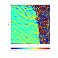 Map of (0 1 0) d-spacing
 -
 Map of XX component of strain tensor
 -
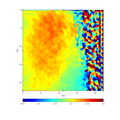 Map of X component of displacement vector


See also
References
- ^ Klinger, Miloslav (2017-07-07). "More features, more tools, more CrysTBox". Journal of Applied Crystallography. 50 (4). International Union of Crystallography (IUCr): 1226–1234. doi:10.1107/s1600576717006793. ISSN 1600-5767.
- ^ "CrysTBox - Crystallographic Toolbox". Fyzikální ústav Akademie věd České republiky. 2021-11-16.
- ^ Dave Mitchell (2022-02-05). "Ellipse fitting analysis".
- ^ Klinger, Miloslav; Polívka, Leoš; Jäger, Aleš; Tyunina, Marina (2016-04-12). "Quantitative analysis of structural inhomogeneity in nanomaterials using transmission electron microscopy". Journal of Applied Crystallography. 49 (3). International Union of Crystallography (IUCr): 762–770. doi:10.1107/s1600576716003800. ISSN 1600-5767.
- ^ Hÿtch, M.J. (1997). "Geometric phase analysis of high resolution electron microscope images". Scanning Microscopy. 11: 53–66.
- ^ Hÿtch, M.J.; Snoeck, E.; Kilaas, R. (1998). "Quantitative measurement of displacement and strain fields from HREM micrographs". Ultramicroscopy. 74 (3). Elsevier BV: 131–146. doi:10.1016/s0304-3991(98)00035-7. ISSN 0304-3991.