List of integrated circuit package dimensions
This article is missing information about Error: you must specify what information is missing.. (January 2013) |
Various form factors are used in integrated circuit packaging, some of which are described below.
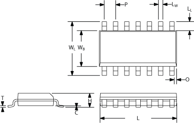
Dimension reference
Surface-mount

C - Clearance between IC body and PCB
H - Total Height
T - Lead Thickness
L - Total Carrier Length
LW - Lead Width
LL - Lead Length
P - Pitch
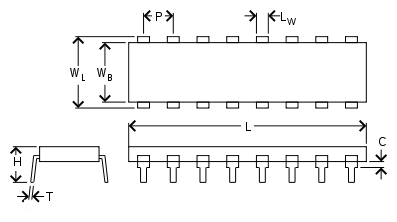
Through hole

C - Clearance between IC body and board
H Total Height
T - Lead Thickness
L - Total Carrier Length
LW - Lead Width
LL - Lead Length
P - Pitch
WB - IC Body Width
WL - Lead-to-Lead Width-
Package dimensions
All measurements below are given in mm. To convert mm to thou, divide mm by 0.0254 (i.e., 2.54 mm / 0.0254 = 100 thou).
- C - Clearance between package body and PCB.
- H - Height of package from pin tip to top of package.
- T - Thickness of pin.
- L - Length of package body only.
- LW - Pin width.
- LL - Pin length from package to pin tip.
- P - Pin pitch (distance between conductors to the PCB).
- WB - Width of the package body only.
- WL - Length from pin tip to pin tip on the opposite side.
Dual row
| Image | Family | Pin | Name | Package | WB | WL | H | C | L | P | LL | T | LW |
|---|---|---|---|---|---|---|---|---|---|---|---|---|---|
 |
DIP | Y | Dual Inline Package | 8-DIP | 6.2-6.48 | 7.62 | 7.7 | 9.2-9.8 | 2.54 (1/10 inch) | 3.05-3.6 | 1.14-1.73 | ||
| 32-DIP | 15.24 | 2.54 (1/10 inch) | |||||||||||
| LFCSP | N | Lead Frame Chip Scale Package | 0.5 | ||||||||||
 |
MSOP | Y | Mini Small Outline Package | 8-MSOP | 3 | 4.9 | 1.1 | 0.10 | 3 | 0.65 | 0.95 | 0.18 | 0.17 - 0.27 |
| 10-MSOP | 3 | 4.9 | 1.1 | 0.10 | 3 | 0.5 | 0.95 | 0.18 | 0.17 - 0.27 | ||||
| 16-MSOP | 3 | 4.9 | 1.1 | 0.10 | 4.04 | 0.5 | 0.95 | 0.18 | 0.17 - 0.27 | ||||
 |
SO SOIC SOP |
Y | Small Outline Integrated Circuit | 8-SOIC | 3.9 | 5.8-6.2 | 1.72 | 0.10-0.25 | 4.8-5.0 | 1.27 | 1.05 | 0.19-0.25 | 0.39-0.46 |
| 14-SOIC | 3.9 | 5.8-6.2 | 1.72 | 0.10-0.25 | 8.55-8.75 | 1.27 | 1.05 | 0.19-0.25 | 0.39-0.46 | ||||
| 16-SOIC | 3.9 | 5.8-6.2 | 1.72 | 0.10-0.25 | 9.9-10 | 1.27 | 1.05 | 0.19-0.25 | 0.39-0.46 | ||||
| 16-SOIC | 7.5 | 10.00-10.65 | 2.65 | 0.10-0.30 | 10.1-10.5 | 1.27 | 1.4 | 0.23-0.32 | 0.38-0.40 | ||||
 |
SOT | Y | Small Outline Transistor | SOT-23-8 | 1.6 | 2.8 | 1.45 | 2.9 | 0.95 | 0.6 | 0.22-0.38 | ||
| SSOP | Y | Shrink Small-Outline Package | |||||||||||
| TDFN | N | Thin Dual Flat No-lead | 8-TDFN | 3 | 3 | 0.7-0.8 | 3 | 0.65 | N/A | 0.19-0.3 | |||
| TSOP | Y | Thin Small-Outline Package | |||||||||||
| TSSOP | Y | Thin Shrink Small Outline Package | 8-TSSOP | 4.4 | 6.4 | 1.2 | 0.15 | 3 | 0.65 | 0.09-0.2 | 0.19-0.3 | ||
| µSOP | Y | Micro Small Outline Package[1] | µSOP-8 | 4.9 | 1.1 | 3 | 0.65 | ||||||
| US8[2] | Y | US8 Package | 2.3 | 3.1 | .7 | 2 | .5 |
Quad rows
| Image | Family | Pin | Name | Package | WB | WL | H | C | L | P | LL | T | LW |
|---|---|---|---|---|---|---|---|---|---|---|---|---|---|
 |
PLCC | N | Plastic Leaded Chip Carrier | 1.27 | |||||||||
| CLCC | N | Ceramic Leadless Chip Carrier | 48-CLCC | 14.22 | 14.22 | 2.21 | 14.22 | 1.016 | N/A | 0.508 | |||
| LQFP | Y | Low-profile Quad Flat Package | |||||||||||
 |
TQFP | Y | Thin Quad Flat Package | TQFP-44 | 10.00 | 12.00 | 0.35-0.50 | 0.80 | 1.00 | 0.09-0.20 | 0.30-0.45 | ||
| TQFN | N | Thin Quad Flat No-lead |
LGA
| Package | x | y | z |
|---|---|---|---|
| 52-ULGA | 12mm | 17mm | .65mm |
| 52-ULGA | 14mm | 18mm | .10mm |
| 52-VELGA | ? | ? | ? |
See also
- List of integrated circuit packaging types
- Surface-mount technology
- three-dimensional integrated circuit
References
- ^ http://pdfserv.maximintegrated.com/package_dwgs/21-0036.PDF
- ^ "Fairchild's TinyLogic family overview" (PDF). March 22, 2013.
External links
Wikimedia Commons has media related to Electronic component packages.
- JEDEC JEP95 official list of all (over 500) standard electronic packages
- Intersil packaging information
- ICpackage.org
- Solder Pad Layout Dimensions
- International Microelectronics And Packaging Society
- The Component Package Database
