
Semiconductor
This article may be too technical for most readers to understand. (August 2011) |
A semiconductor is a material which has electrical conductivity between that of a conductor such as copper and an insulator such as glass. The conductivity of a semiconductor increases with increasing temperature, behaviour opposite to that of a metal.[1] Semiconductors can display a range of useful properties such as passing current more easily in one direction than the other. Because the conductive properties of a semiconductor can be modified by controlled addition of impurities or by the application of electrical fields or light, semiconductors are very useful devices for amplification of signals, switching, and energy conversion. Understanding the properties of semiconductors relies on quantum physics to explain the motions of electrons through a lattice of atoms.
Current conduction in a semiconductor occurs via free electrons and "holes", collectively known as charge carriers. Adding impurity atoms to a semiconducting material, known as "doping", greatly increases the number of charge carriers within it. When a doped semiconductor contains excess holes it is called "p-type", and when it contains excess free electrons it is known as "n-type". The semiconductor material used in devices is doped under highly controlled conditions to precisely control the location and concentration of p- and n-type dopants. A single semiconductor crystal can have multiple p- and n-type regions; the p–n junctions between these regions have many useful electronic properties and characteristics.
Semiconductors are the foundation of modern electronics, including radio, computers, and telephones. Semiconductor-based electronic components include transistors, solar cells, many kinds of diodes including the light-emitting diode (LED), the silicon controlled rectifier, photo-diodes, and digital and analog integrated circuits. Increasing understanding of semiconductor materials and fabrication processes has made possible continuing increases in the complexity and speed of semiconductor devices, an effect known as Moore's law.
History
The history of the understanding of semiconductors begins with experiments on the electrical properties of materials. The properties of negative temperature coefficient of resistance, rectification, and light-sensitivity were observed starting in the early 19th century.
In 1833, Michael Faraday reported that the resistance of specimens of silver sulfide decreases when they are heated. This is contrary to the behavior of metallic substances such as copper. In 1839, A. E. Becquerel reported observation of a voltage between a solid and a liquid electrolyte when struck by light, the photovoltaic effect. In 1873 Willoughby Smith observed that selenium resistors exhibit decreasing resistance when light falls on them. In 1874 Karl Ferdinand Braun observed conduction and rectification in metallic sulphides, and Arthur Schuster found that a copper oxide layer on wires has rectification properties that ceases when the wires are cleaned. Adams and Day observed the photovoltaic effect in selenium in 1876.[2]
A unified explanation of these phenomena required a theory of solid state physics which developed greatly in the first half of the 20th Century. In 1878 Edwin Herbert Hall demonstrated the deflection of flowing charge carriers by an applied magnetic field, the Hall effect. The discovery of the electron by J.J. Thomson in 1897 prompted theories of electron-based conduction in solids. Karl Baedeker, by observing a Hall effect with the reverse sign to that in metals, theorized that copper iodide had positive charge carriers. Johan Koenigsberger classified solid materials as metals, insulators and "variable conductors" in 1914. Felix Bloch published a theory of the movement of electrons through atomic lattices in 1928. In 1930, B. Gudden stated that conductivity in semiconductors was due to minor concentrations of impurities. By 1931, the band theory of conduction had been established by Alan Herries Wilson and the concept of band gaps had been developed. Walter H. Schottky and Nevill Francis Mott developed models of the potential barrier and of the characteristics of a metal-semiconductor junction. By 1938, Boris Davydov had developed a theory of the copper-oxide rectifer, identifying the effect of the p–n junction and the importance of minority carriers and surface states.[3]
Agreement between theoretical predictions (based on developing quantum mechanics) and experimental results was sometimes poor. This was later explained by John Bardeen as due to the extreme "structure sensitive" behavior of semiconductors, whose properties change dramatically based on tiny amounts of impurities.[3] Commercially pure materials of the 1920s containing varying proportions of trace contaminants produced differing experimental results. This spurred the development of improved material refining techniques, culminating in modern semiconductor refineries producing materials with parts-per-trillion purity.
Devices using semiconductors at first were constructed based on empirical knowledge, but semiconductor theory provided a guide to construction of more capable and reliable devices.
Alexander Graham Bell used the light-sensitive property of selenium to Photophone transmit sound over a beam of light in 1880. A working solar cell, of low efficiency, was constructed by Charles Fritts in 1883 using a metal plate coated with selenium and a thin layer of gold; the device became commercially useful in photographic light meters in the 1930s.[3] Point-contact microwave detector rectifiers made of lead sulfide were used by Jagadish Chandra Bose in 1904; the cat's-whisker detector using natural galena or other materials became a common device in the development of radio. However, it was somewhat unpredictable in operation and required manual adjustment for best performance. In 1906 H.J. Round observed light emission when electric current passed through silicon carbide crystals, the principle behind the light emitting diode. Oleg Losev observed similar light emission in 1922 but at the time the effect had no practical use. Power rectifiers, using copper oxide and selenium, were developed in the 1920s and became commercially important as an alternative to vacuum tube rectifiers.[2][3]
In the years preceding World War II, infra-red detection and communications devices prompted research into lead-sulfide and lead-selenide materials. These devices were used for detecting ships and aircraft, for infrared rangefinders, and for voice communication systems. The point-contact crystal detector became vital for microwave radio systems, since available vacuum tube devices could not serve as detectors above about 4000 MHz; advanced radar systems relied on the fast response of crystal detectors. Considerable research and development of silicon materials occurred during the war to develop detectors of consistent quality.[3]
Detector and power rectifiers could not amplify a signal. Many efforts were made to develop a solid-state amplifier, but these were unsuccessful because of limited theoretical understanding of semiconductor materials.[3] In 1922 Oleg Losev developed two-terminal, negative resistance amplifiers for radio; however, he perished in the Siege of Leningrad. In 1926 J.E. Lilenfeld patented a device resembling a modern field-effect transistor, but it was not practical. R. Hilsch and R. W. Pohl in 1938 demonstrated a solid-state amplifier using a structure resembling the control grid of a vacuum tube; although the device displayed power gain, it had a cut-off frequency of one cycle per second, too low for any practical applications, but an effective application of the available theory.[3] At Bell Labs, William Shockley and A. Holden started investigating solid-state amplifiers in 1938. The first p–n junction in silicon was observed by Russell Ohl about 1941, when a specimen was found to be light-sensitive, with a sharp boundary between p-type impurity at one end and n-type at the other. A slice cut from the specimen at the p–n boundary developed a voltage when exposed to light.
In France, during the war, Herbert Mataré had observed amplification between adjacent point contacts on a germanium base. After the war, Mataré's group announced their "Transistron" amplifier only shortly after Bell Labs announced the "transistor".
Materials
A large number of elements and compounds have semiconducting properties, including:[1]
- Certain pure elements found in Group IV of the periodic table; the most commercially important of these elements are silicon and germanium.
- Binary compounds, particularly between elements in Groups III and V, such as gallium arsenide, Groups II and VI, groups IV and VI, and between different group IV elements, e.g. silicon carbide.
- Certain ternary compounds, oxides and alloys.
- A number of organic compounds.
An intrinsic semiconductor is made up of one pure element or pure compound. At room temperature, the conductivity of intrinsic semiconductors is relatively low because there are very few charge carriers available. Conductivity is greatly enhanced by a process called doping, in which very small amounts of other elements are added to the intrinsic crystal to create what is called an extrinsic semiconductor.
Most common semiconducting materials are crystalline solids, but amorphous and liquid semiconductors are also known. These include hydrogenated amorphous silicon and mixtures of arsenic, selenium and tellurium in a variety of proportions. These compounds share with better known semiconductors the properties of intermediate conductivity and a rapid variation of conductivity with temperature, as well as occasional negative resistance. Such disordered materials lack the rigid crystalline structure of conventional semiconductors such as silicon. They are generally used in thin film structures, which do not require material of higher electronic quality, being relatively insensitive to impurities and radiation damage.
Energy bands and electrical conduction
Semiconductors are defined by their unique electric conductive behavior. Metals are good conductors because at their Fermi level, there is a large density of energetically available states that each electron can occupy. Electrons can move quite freely between energy levels without a high energy cost. Metal conductivity decreases with temperature increase because thermal vibrations of crystal lattice disrupt the free motion of electrons. Insulators, by contrast, are very poor conductors of electricity because there is a large difference in energies (called a band gap) between electron-occupied energy levels and empty energy levels that allow for electron motion.
Insulator conductivity increases with temperature because heat provides energy to promote electrons across the band gap to the higher electron conduction energy levels (called the conduction band). Semiconductors, on the other hand, have an intermediate level of electric conductivity when compared to metals and insulators. Their band gap is small enough that small increase in temperature promotes sufficient number of electrons (to result in measurable currents) from the lowest energy levels (in the valence band) to the conduction band. This creates electron holes, or unoccupied levels, in the valence band, and very loosely held electrons in the conduction band.[4][5]

In the classic crystalline semiconductors, electrons can have energies only within certain bands (ranges). The range of energy runs from the ground state, in which electrons are tightly bound to the atom, up to a level where the electron can escape entirely from the material. Each energy band corresponds to a large number of discrete quantum states of the electrons. Most of the states with low energy (closer to the nucleus) are occupied, up to the valence band.
Semiconductors and insulators are distinguished from metals by the population of electrons in each band. The valence band in any given metal is nearly filled with electrons under usual conditions, and metals have many free electrons with energies in the conduction band. In semiconductors, only a few electrons exist in the conduction band just above the valence band, and an insulator has almost no free electrons.
The ease with which electrons in the semiconductor can be excited from the valence band to the conduction band depends on the band gap. The size of this energy gap (bandgap) determines whether a material is semiconductor or an insulator (nominally this dividing line is roughly 4 eV).
With covalent bonds, an electron moves by hopping to a neighboring bond. The Pauli exclusion principle requires the electron to be lifted into the higher anti-bonding state of that bond. For delocalized states, for example in one dimension – that is in a nanowire, for every energy there is a state with electrons flowing in one direction and another state with the electrons flowing in the other. For a net current to flow, more states for one direction than for the other direction must be occupied. For this to occur, energy is required, as in the semiconductor the next higher states lie above the band gap. Often this is stated as: full bands do not contribute to the electrical conductivity. However, as the temperature of a semiconductor rises above absolute zero, there is more energy in the semiconductor to spend on lattice vibration and on exciting electrons into the conduction band.
Electrons excited to the conduction band also leave behind electron holes, i.e. unoccupied states in the valence band. Both the conduction band electrons and the valence band holes contribute to electrical conductivity. The holes themselves don't move, but a neighboring electron can move to fill the hole, leaving a hole at the place it has just come from, and in this way the holes appear to move, and the holes behave as if they were actual positively charged particles.
One covalent bond between neighboring atoms in the solid is ten times stronger than the binding of the single electron to the atom, so freeing the electron does not imply destruction of the crystal structure.
Explaining energy bands
The theory of electron energy levels in solids is an application of the principles of quantum mechanics. In principle, the motions of electrons can be predicted by solution of Schrödinger's equation for the potential field of a particular arrangement of atoms in a crystal. Since a general solution is quite difficult, various simplifying assumptions are used to represent the actual system.
A fundamental observation leading to the development of quantum mechanics is that the energy levels of an electron around an atom do not vary continuously, but instead occurs in discrete quantum states called "orbitals", each associated with an amount of energy. Another observation, stated as the Pauli exclusion principle, is that no two electrons can occupy exactly the same quantum state; so, not all the electrons of the atom fall into the lowest state, but occupy increasingly energetic "shells" around the atom.
Putting two atoms together leads to delocalized orbitals across two atoms, yielding a partially covalent bond. Additional quantum states are possible, in this molecular orbital, with different energy levels.
In a crystal, many atoms are adjacent and many energy levels are possible for electrons. Since there are so many (on the order of 1022) atoms in a macroscopic crystal, the resulting energy states available for electrons are very closely spaced. Since the Heisenberg principle limits the precision of any measurement of the combination of an electron's momentum (related to energy) and its position, in a crystal effectively the available energy levels form a continuous band of allowed energy levels.
The mathematical solution of the Schrödinger equation gives two kinds of solutions depending on the energy of the electrons. One type of solution represents an electron moving indefinitely through the crystal as a plane wave; the particular solutions for a periodic regular crystal lattice are called Bloch functions. A second type of solution occurs for energy levels in the so-called "forbidden" gaps between "allowed" states - in this case, the electron cannot travel indefinitely through the crystal with that energy and will either be reflected at the edges of the region, or possibly must pass through the region in a phenomenon called "quantum tunnelling".
For semiconductor materials, one band of "allowed" electron energies is called the "valence band" - these can be thought of electrons bound to a particular atom. A higher-energy band is called the "conduction band", where electrons may travel through the crystal.[6] The energy of an electron may be increased by increasing its temperature or by applying an electric field to it. If a band of allowable energies is completely filled by electrons, it cannot carry any electrical current, because that would require the electron's energy to be increased. Conduction can only occur with partially filled bands.
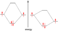
The Fermi energy plays an important role in describing the behavior of doped semiconductors. A substance’s Fermi energy is defined as the highest occupied energy level found in that substance at absolute zero temperature (0 kelvins or -273 °C). At higher temperatures, energy from heat is available to promote electrons into slightly higher energy levels. However, picturing the density of states to be filled to the Fermi energy helps scientists understand different behaviors between insulators, metals, and intrinsic and extrinsic semiconductors. As seen in Figure 1 (below), the Fermi energy of n-type semiconductors is elevated from that of the corresponding un-doped intrinsic semiconductor. This makes the conduction band much more thermally accessible at temperatures above absolute zero.[5]

The Fermi level is the energy below which there is a 50% chance of finding an occupied energy state. The Fermi level can be calculated from the density of states in the conduction and valence bands. The Fermi level may increase, remain the same or decrease with increasing temperature, depending on the number of states in the conduction and valence bands. Where two regions with different Fermi levels are in contact, charge carriers will flow between the two regions until the Fermi level is aligned across the interface.
At absolute zero temperature the Fermi level can be thought of as the energy up to which available electron states are occupied. At higher temperatures, the Fermi level is the energy at which the probability of a state being occupied has fallen to 0.5.
- atoms – crystal – vacuum
-
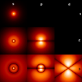 In a single H-atom an electron resides in orbitals labelled s, p, d in order of increasing energy.
 -
 Putting two atoms together leads to delocalized orbitals across two atoms, yielding a partially covalent bond. Due to the Pauli exclusion principle, every state can contain only one electron.
 -
 This can be continued with more atoms. Note: This picture shows a metal, not a semiconductor.
 -
 Continuing to add atoms creates a crystal.
 -
 For this regular solid the band structure can be calculated or measured.
 -
 Integrating over the k axis gives the bands of a semiconductor showing a full valence band and an empty conduction band. Generally stopping at the vacuum level is undesirable, because some people want to calculate: photoemission, inverse photoemission


Holes: electron absence as a charge carrier
The concept of holes can also be applied to metals, where the Fermi level lies within the conduction band. With most metals the Hall effect indicates electrons are the charge carriers. However, some metals have a mostly filled conduction band. In these, the Hall effect reveals positive charge carriers, which are not the ion-cores, but holes. In the case of a metal, only a small amount of energy is needed for the electrons to find other unoccupied states to move into, and hence for current to flow. Sometimes even in this case it may be said that a hole was left behind, to explain why the electron does not fall back to lower energies: It cannot find a hole. In the end in both materials electron-phonon scattering and defects are the dominant causes for resistance.

The energy distribution of the electrons determines which of the states are filled and which are empty. This distribution is described by Fermi–Dirac statistics. The distribution is characterized by the temperature of the electrons, and the Fermi level. The dependence of the electron energy distribution on temperature also explains why the conductivity of a semiconductor has a strong temperature dependency, as a semiconductor operating at lower temperatures will have fewer available free electrons and holes able to do the work.
Energy–momentum dispersion
In the preceding description an important fact is ignored for the sake of simplicity: the dispersion of the energy. The reason that the energies of the states are broadened into a band is that the energy depends on the value of the wave vector, or k-vector, of the electron. The k-vector, in quantum mechanics, is the representation of the momentum of a particle.
The dispersion relationship determines the effective mass, m*, of electrons or holes in the semiconductor, according to the formula:
![{\displaystyle m^{*}=\hbar ^{2}\cdot \left[{{d^{2}E(k)} \over {dk^{2}}}\right]^{-1}.}](https://wikimedia.org/api/rest_v1/media/math/render/svg/39a763b076be5dee484033585ff2549d548570b5)
The effective mass is important as it affects many of the electrical properties of the semiconductor, such as the electron or hole mobility, which in turn influences the diffusivity of the charge carriers and the electrical conductivity of the semiconductor.
Typically the effective mass of electrons and holes are different. This affects the relative performance of p-channel and n-channel IGFETs.[7]
The top of the valence band and the bottom of the conduction band might not occur at that same value of k. Materials with this situation, such as silicon and germanium, are known as indirect bandgap materials. Materials in which the band extrema are aligned in k, for example gallium arsenide, are called direct bandgap semiconductors. Direct gap semiconductors are particularly important in optoelectronics because they are much more efficient as light emitters than indirect gap materials; an electron moving between two bands need not exchange momentum with phonons in the crystal lattice.
Carrier generation and recombination
When ionizing radiation strikes a semiconductor, it may excite an electron out of its energy level and consequently leave a hole. This process is known as electron–hole pair generation. Electron-hole pairs are constantly generated from thermal energy as well, in the absence of any external energy source.
Electron-hole pairs are also apt to recombine. Conservation of energy demands that these recombination events, in which an electron loses an amount of energy larger than the band gap, be accompanied by the emission of thermal energy (in the form of phonons) or radiation (in the form of photons).
In some states, the generation and recombination of electron–hole pairs are in equipoise. The number of electron-hole pairs in the steady state at a given temperature is determined by quantum statistical mechanics. The precise quantum mechanical mechanisms of generation and recombination are governed by conservation of energy and conservation of momentum.
As the probability that electrons and holes meet together is proportional to the product of their amounts, the product is in steady state nearly constant at a given temperature, providing that there is no significant electric field (which might "flush" carriers of both types, or move them from neighbour regions containing more of them to meet together) or externally driven pair generation. The product is a function of the temperature, as the probability of getting enough thermal energy to produce a pair increases with temperature, being approximately exp(−EG/kT), where k is Boltzmann's constant, T is absolute temperature and EG is band gap.
The probability of meeting is increased by carrier traps—impurities or dislocations which can trap an electron or hole and hold it until a pair is completed. Such carrier traps are sometimes purposely added to reduce the time needed to reach the steady state.
Doping
The conductivity of semiconductors may easily be modified by introducing impurities into their crystal lattice. The process of adding controlled impurities to a semiconductor is known as doping. The amount of impurity, or dopant, added to an intrinsic (pure) semiconductor varies its level of conductivity. Doped semiconductors are referred to as extrinsic. By adding impurity to pure semiconductors, the electrical conductivity may be varied by factors of thousands or millions.
A 1 cm3 specimen of a metal or semiconductor has of the order of 1022 atoms. In a metal, every atom donates at least one free electron for conduction, thus 1 cm3 of metal contains on the order of 1022 free electrons. Whereas a 1 cm3 of sample pure germanium at 20 °C, contains about 4.2×10²² atoms but only 2.5×10¹³ free electrons and 2.5×10¹³ holes. The addition of 0.001% of arsenic (an impurity) donates an extra 1017 free electrons in the same volume and the electrical conductivity is increased by a factor of 10,000.
The materials chosen as suitable dopants depend on the atomic properties of both the dopant and the material to be doped. In general, dopants that produce the desired controlled changes are classified as either electron acceptors or donors. Semiconductors doped with donor impurities are called n-type, while those doped with acceptor impurities are known as p-type. The n and p type designations indicate which charge carrier acts as the material's majority carrier. The opposite carrier is called the minority carrier, which exists due to thermal excitation at a much lower concentration compared to the majority carrier.
For example, the pure semiconductor silicon has four valence electrons which bond each silicon atom to its neighbors. In silicon, the most common dopants are group III and group V elements. Group III elements all contain three valence electrons, causing them to function as acceptors when used to dope silicon. When an acceptor atom replaces a silicon atom in the crystal, a vacant state ( an electron "hole") is created, which can move around the lattice and functions as a charge carrier. Group V elements have five valence electrons, which allows them to act as a donor; substitution of these atoms for silicon creates an extra free electron. Therefore, a silicon crystal doped with boron creates a p-type semiconductor whereas one doped with phosphorus results in an n-type material.
During manufacture, dopants can be diffused into the semiconductor body by contact with gaseous compounds of the desired element, or ion implantation can be used to accurately position the doped regions.
Preparation of semiconductor materials
Semiconductors with predictable, reliable electronic properties are necessary for mass production. The level of chemical purity needed is extremely high because the presence of impurities even in very small proportions can have large effects on the properties of the material. A high degree of crystalline perfection is also required, since faults in crystal structure (such as dislocations, twins, and stacking faults) interfere with the semiconducting properties of the material. Crystalline faults are a major cause of defective semiconductor devices. The larger the crystal, the more difficult it is to achieve the necessary perfection. Current mass production processes use crystal ingots between 100 mm and 300 mm (4–12 inches) in diameter which are grown as cylinders and sliced into wafers.
Because of the required level of chemical purity and the perfection of the crystal structure which are needed to make semiconductor devices, special methods have been developed to produce the initial semiconductor material. A technique for achieving high purity includes growing the crystal using the Czochralski process. An additional step that can be used to further increase purity is known as zone refining. In zone refining, part of a solid crystal is melted. The impurities tend to concentrate in the melted region, while the desired material recrystalizes leaving the solid material more pure and with fewer crystalline faults.
In manufacturing semiconductor devices involving heterojunctions between different semiconductor materials, the lattice constant, which is the length of the repeating element of the crystal structure, is important for determining the compatibility of materials.
Organic materials
Organic semiconductors have been of great research interest for use in low cost, ultra thin, and flexible products such as displays and solar cells. While many p-type organic semiconductors have been thoroughly characterized, n-type organic semiconductors have proven hard to obtain. Both types are needed for the diodes and transistors that make desirable devices possible. N-type organic semiconductors were produced of the arylene diimide family that are resistant to thermal and environmental stresses, which is one of the largest challenges in the field.[8] Several other compounds are being explored for n-type organic semiconductors for use in organic field-effect transistors (OFET), such as fullerene (C60) and chemically modified oligothiophenes. Semiconductors are made from these compounds by reduction with electron withdrawing groups or, alternatively, by modifying the surface properties to control electron trapping.[9] Organic thin film transistors (OTFTs) are being explored because their low synthesis temperatures allow them to be deposited on thin plastic substrates without damage, resulting in thin and flexible devices. Same compounds are often considered for use in OFETs and OTFTs.[10]
Semi-insulators
Some wider-band gap semiconductor materials are sometimes referred to as semi-insulators. These have electrical conductivity nearer to that of electrical insulators. Semi-insulators find niche applications in micro-electronics, such as substrates for HEMT. An example of a common semi-insulator is gallium arsenide.[11] Some materials, such as titanium dioxide, can even be used as insulating materials for some applications, while being treated as wide-gap semiconductors for other applications.
See also
- Exciton
- Luttinger parameter
- Semiconductor industry
- Thin film
- Tight-binding model
- Semiconductor characterization techniques
References
- ^ a b B.G. Yacobi, Semiconductor Materials: An Introduction to Basic Principles, Springer 2003 ISBN 0306473615, pp. 1-3
- ^ a b http://www.nit.eu/czasopisma/JTIT/2010/1/3.pdf Lidia Łukasiak and Andrzej Jakubowski, History of Semiconductors in Journal of Telecommunication and Information Technology1/2010
- ^ a b c d e f g Peter Robin Morris A History of the World Semiconductor Industry, IET 1990, ISBN 0863412270, pp.11-25
- ^ Smart, L.; et al. (2005). State Chemistry: An Introduction. pp. 165–171. ISSN 0-7487-7516-1.
{{cite book}}: Check|issn=value (help); Explicit use of et al. in:|author=(help) - ^ a b Miessler, G.; et al. (1965). Inorganic Chemistry (3rd ed.). pp. 237–240. ISSN 0-7487-7516-1.
{{cite book}}: Check|issn=value (help); Explicit use of et al. in:|author=(help) - ^ Robert L. Sproull, Modern Physics:The quantum physics of atoms, solids and and nuclei, Second Edition, John Wiley and Sons, 1963 ISBN 0-471- 8145-3 Chapter 8
- ^ Muller, Richard S. (1986). Device Electronics for Integrated Circuits (2d ed.). New York: Wiley. p. 427. ISBN 0-471-88758-7.
{{cite book}}: Unknown parameter|coauthors=ignored (|author=suggested) (help) - ^ Jones, B.; et al. (2007). "Tuning Orbital Energetics in Arylene Diimide Semiconductors". Prog J. Am. Chem. Soc. 129: 15259–15278. doi:10.1021/ja075242e.
{{cite journal}}: Explicit use of et al. in:|author=(help) - ^ Facchetti, A. (2007). "Semiconductors for organic transistors". Materials Today. 10 (3): 29–37. ISSN 1369-7021.
- ^ Newman, C.; et al. (2004). "Introduction to Organic Thin Film Transistors". Chem. Mater. 16: 4436–4451. doi:10.1021/cm049391x.
{{cite journal}}: Explicit use of et al. in:|author=(help) - ^ J. W. Allen (1960). "Gallium Arsenide as a semi-insulator". Nature. 187 (4735): 403–405. Bibcode:1960Natur.187..403A. doi:10.1038/187403b0.
Further reading
- A. A. Balandin and K. L. Wang (2006). Handbook of Semiconductor Nanostructures and Nanodevices (5-Volume Set). American Scientific Publishers. ISBN 1-58883-073-X.
- Sze, Simon M. (1981). Physics of Semiconductor Devices (2nd ed.). John Wiley and Sons (WIE). ISBN 0-471-05661-8.
- Turley, Jim (2002). The Essential Guide to Semiconductors. Prentice Hall PTR. ISBN 0-13-046404-X.
- Yu, Peter Y.; Cardona, Manuel (2004). Fundamentals of Semiconductors : Physics and Materials Properties. Springer. ISBN 3-540-41323-5.
{{cite book}}: CS1 maint: multiple names: authors list (link) - Sadao Adachi (2012). The Handbook on Optical Constants of Semiconductors: In Tables and Figures. World Scientific Publishing. ISBN 9-789-81440597-3.
External links
- Howstuffworks' semiconductor page
- Semiconductor Concepts at Hyperphysics
- Calculator for the intrinsic carrier concentration in silicon
- Semiconductor OneSource Hall of Fame, Glossary
- Principles of Semiconductor Devices by Bart Van Zeghbroeck, University of Colorado. An online textbook]
- US Navy Electrical Engineering Training Series
- NSM-Archive Physical Properties of Semiconductors]
- Semiconductor Manufacturer List
- ABACUS : Introduction to Semiconductor Devices – by Gerhard Klimeck and Dragica Vasileska, online learning resource with simulation tools on nanoHUB
- Organic Semiconductor page
- DoITPoMS Teaching and Learning Package- "Introduction to Semiconductors"
- Semiconductor R&D Talent Locations report