Radeon R400 series
| Release date | 2004–2005 |
|---|---|
| Codename | Loki |
| Architecture | Radeon R400 |
| Cards | |
| Entry-level | None |
| Mid-range | X700, X740 |
| High-end | X800 |
| Enthusiast | X850 |
| API support | |
| DirectX | Direct3D 9.0b Shader Model 2.0b |
| OpenGL | OpenGL 2.0 |
| History | |
| Predecessor | Radeon 9000 Series Radeon X300 Series Radeon X500 Series Radeon X600 Series |
| Successor | Radeon X1000 Series |
The R420 GPU, developed by ATI Technologies, was the company's basis for its 3rd-generation DirectX 9.0/OpenGL 2.0-capable graphics cards. Used first on the Radeon X800, the R420 was produced on a 0.13 micrometer (130 nm) low-K photolithography process and used GDDR-3 memory. The chip was designed for AGP graphics cards.
Driver support of this core was discontinued as of Catalyst 9.4, and as a result there is no official Windows 7 support for any of the X700 - X850 products.[1]
Development
In terms of supported DirectX features, R420 (codenamed Loki) was very similar to the R300. R420 basically takes a "wider is better" approach to the previous architecture, with some small tweaks thrown in to enhance it in various ways. The chip came equipped with over double the pixel and vertex pushing resources compared to the Radeon 9800 XT's R360 (a minor evolution of the R350), with 16 DirectX 9.0b pixel pipelines and 16 ROPs. One would not be far off seeing the X800 XT basically as a pair of Radeon 9800 cores connected together and also running with a ~30% higher clock speed.
The R420 design was a 4 "quad" arrangement (4 pipelines per quad.) This organization internally allowed ATI to disable defective "quads" and sell chips with 12, 8 or even 4 pixel pipelines, an evolution of the technique used with Radeon 9500/9700 and 9800SE/9800. The separation into "quads" also allowed ATI to design a system to optimize the efficiency of the overall chip. Coined the "quad dispatch system", the screen is tiled and work is spread out evenly among the separate "quads" to optimize their throughput. This is how the R300-series chips performed their tasks as well, but R420 refined this by allowing programmable tile sizes in order to control work flow on a finer level of granularity. Apparently by reducing tile sizes, ATI was able to optimize for different triangle sizes.
When ATI doubled the number of pixel pipelines, they also raised the number of vertex shader engines from 4 to 6. This changed the ratio of pixel/vertex shaders from 2:1 (on R300) to 8:3, showing that ATI believed the workload in games as of 2004 and onward to be more pixel shader and texturing oriented than geometry based. Normal and parallax mapping were replacing sheer geometric complexity for model detail, so undoubtedly that was part of the reasoning. Strangely, the X700 mainstream card (RV410) had 6 vertex shaders while only being equipped with 2 quads. As such, this chip was obviously designed for a heavier geometry load than texturing, perhaps being tailored for a role as a FireGL chip. RV410 also significantly outgunned NVIDIA's GeForce 6600GT (3 vertex shaders) on geometry throughput. With R420's and RV410's 6 vertex shaders combined with higher clock speeds than the previous generation, ATI was able to more than double the geometry processing capability of 9800XT.
Although the R420-based chips are fundamentally similar to R300-based cores, ATI did tweak and enhance the pixel shader units for more flexibility. A new pixel shader version (PS2.b) allowed slightly greater shader program flexibility than plain PS2.0, but was still shy of full PS3.0 capabilities. This new revision to PS2.0 increased the maximum number of instructions and registers available to pixel shader programs.[2]
ATI revealed Temporal Anti-Aliasing, a new anti-aliasing technology their chips were capable of. By taking advantage of the frame-to-eye effects of a framerate higher than 60 frame/s, the GPU is able to better smooth aliased edges by rotating the anti-aliasing sampling pattern between frames. A 2X software setting became perceptively equivalent to 4X. Unfortunately, it required the system to be able to maintain at least 60 frame/s or temporal anti-aliasing would cause a noticeable flickering, because the user would be able to see the alternating AA patterns. If the framerate could not be maintained, the driver will disable Temporal AA. However, in games which this performance level could be maintained, Temporal AA was a nice addition to ATI's excellent anti-aliasing options. Note, ATI's "Temporal AA" was actually a temporal dithering filter for spatial AA, not de facto temporal anti-aliasing (which must involve a controlled blending of the temporal subsamples from consecutive screens).

Another notable addition to the core was a new kind of normal map compression, dubbed "3Dc". Similar to how texture compression had been part of the Direct3D specification for years and was used for compressing regular textures, normal map compression compacted this new type of surface detail layer. Because DirectX Texture Compression (DXTC) was block-based and not designed for a normal map's different data properties, a new compression method was needed to prevent loss of detail and other artifacting. 3Dc was based on a modified DXT5 mode, which in fact was a fallback option for hardware not supporting 3Dc. Software making heavy use of normal mapping could gain a significant speed boost from the savings in fillrate and bandwidth by using 3Dc. ATI showcased many of their chip's new features in the promotional real-time demo called, Ruby: The Doublecross.
Most of the rest of the GPU was extremely similar to R300. The memory controller and memory bandwidth optimization techniques (HyperZ) were identical.
R420 was actually a secondary 4th generation project for ATI, with the original R400 plan being scrapped.[3] R400 would have been more feature-complete, likely with full PS3.0 support among other enhancements, but it is believed that ATI deemed R400 unnecessarily complex for the applications that would be available, and potentially risky to develop on the available semiconductor manufacturing processes of the time.[4] R400 technology was thus moved to the subsequent generation, renamed to "R500" (became "R520"), while the 4th generation was served with the R300-derived R420.
Releases of the R420 and the next ATI GPU without major architecture modification

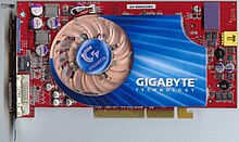
The earliest Radeon X800 series cards were based on the R420 core. The line included the Radeon X800 XT Platinum Edition and the Radeon X800 Pro. The X800 XT PE came clocked at 520 MHz core and 560 MHz RAM, with 16 pipelines enabled. The X800 Pro came clocked at 475/450 MHz with one quad disabled, leaving 12 pixel pipelines functional. Essentially, the X800 Pro is built on semi-defective R420 cores. An X800 Pro VIVO (Video-in-Video-out) was also released and was popular with overclockers because the disabled quad could usually be enabled, resulting in a fully functional X800 XT PE at a lower cost.
The Radeon X700 (RV410) series replaced the X600 in September 2004. X700 Pro is clocked at 425 MHz core, and produced on a 0.11 micrometre process. RV410 used a layout consisting of 8 pixel pipelines connected to 4 ROPs (similar to GeForce 6600) while maintaining the 6 vertex shaders of X800. The 110 nm process was a cost-cutting process, designed not for high clock speeds but for reducing die size while maintaining high yields. An X700 XT was planned for production, and reviewed by various hardware web sites, but was never released. It was believed that X700 XT set too high of a clock ceiling for ATI to profitably produce. X700 XT was also not adequately competitive with nVidia's impressive GeForce 6600GT. ATI would go on produce a card in the X800 series to compete instead.

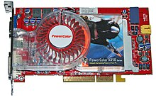
The Radeon X800 "R430"-based 110 nanometer series was introduced at the end of 2004 along with ATI's new X850 cards. The X800 was designed to replace the position X700 XT failed to secure, with 12 pipelines and a 256-bit RAM bus. The card more than surpassed the 6600GT with performance similar to that of the GeForce 6800. A close relative, the new X800 XL, was positioned to dethrone NVIDIA's GeForce 6800 GT with higher memory speeds and a full 16 pipelines to boost performance. R430 was unable to reach high clock speeds, being mainly designed to reduce the cost per GPU, and so a new top-of-the-line core was still needed. The new high-end R4x0-generation arrived with the X850 series, equipped with various core tweaks for slightly higher performance than the "R420"-based X800 series. The "R480"-based X850 line was available in 3 forms: the X850 Pro, the X850 XT, and the X850 XT Platinum Edition, and was built on the reliable high-performance 130 nm Low-K process.
In 2005, ATI had a large number of dies that "worked" but not well enough to be used on the X800 or X850 series cards. So a new SKU was created, the X800 GT. It used any "R480" X850 die or "R430" X800 XL die that had 2 functional quads and could run at 475 MHz. They were meant to compete with the GeForce 6600GT beside the previous "R430"-based X800. ATI also released the X800 GTO, which was a 12 pipeline card (3 quads) using either "R480" or "R430" dies clocked at 400 MHz. This card performed between the X800 GT and the X800 XL. It was faster than the plain GeForce 6800, but slower than GeForce 6800 GT. High sales for this card were due to its relatively high performance coupled with a cost only slightly higher than the X800 GT. The overclocking community discovered that the R480-based GTO could frequently reach clock speeds near the X850 XT.
Finally, another SKU was the X800 GTO², again based on R480. It was again manufactured by Sapphire Technology, like the X800 GTO. This card usually came with a 3 quad configuration, like X800 GTO. The GTO² was unique in the GTx series because, with a BIOS change, they could almost always be turned into a full 4 quad card.[5] Some X800 GTO² cards shipped with the full 4 quads already enabled, but of these some were R430 instead of R480 and weren't able to reach X850-like clock speeds. The final variations of the GTO series were the special GTO boards with 16 pipelines officially enabled, such as Powercolor's "R430"-based X800 GTO-16.
Table of models
References
- ^ "Archived copy". Archived from the original on 2009-05-07. Retrieved 2010-01-04.
{{cite web}}: CS1 maint: archived copy as title (link) - ^ Baumann, Dave. ATI Radeon X800 XT Platinum Edition / PRO Review, Beyond3d.Com, May 4, 2004.
- ^ ATI R400, Endian.net, accessed July 6, 2006.
- ^ What was R400? (thread), Beyond3d.Com forum, November 11, 2004.
- ^ Baxtor, Shane. Unlocking the Sapphire X800 GTO² - 12 vs. 16 Pipe Adventure, Tweaktown.Com, October 20, 2005.
- "Beyond3D: 3D Tables" by Beyond3D.Com, retrieved January 17, 2006
- "Radeon X850 XT Platinum Edition Review" by Dave Baumann, Beyond3D.Com, December 1, 2004, retrieved January 17, 2006
External links
- "Inside ATI's R420 (architectural analysis)" by aths, 3DCenter.Org, May 4, 2004
- ATI's X800 Pulls Off Another Coup in the Graphics Performance War — features, architecture and benchmarks of the Radeon X800
- ATI's Radeon X700 XT graphics card — An in-depth look at the unreleased X700 XT.
- techPowerUp! GPU Database
