Dual-ported video RAM
This article has multiple issues. Please help improve it or discuss these issues on the talk page. (Learn how and when to remove these messages)
|
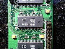
Video RAM, or VRAM, is a dual-ported variant of dynamic RAM (DRAM), which was once commonly used to store the framebuffer in graphics adapters. Note that most computers and game consoles do not use this form of memory, and dual-ported VRAM should not be confused with other forms of video memory.

It was invented by F. Dill, D. Ling and R. Matick at IBM Research in 1980, with a patent issued in 1985 (US Patent 4,541,075).[1] The first commercial use of VRAM was in a high-resolution graphics adapter introduced in 1986 by IBM for its RT PC system, which set a new standard for graphics displays. Prior to the development of VRAM, dual-ported memory was quite expensive, limiting higher resolution bitmapped graphics to high-end workstations. VRAM improved the overall framebuffer throughput, allowing low cost, high-resolution, high-speed, color graphics. Modern GUI-based operating systems benefitted from this and thus it provided a key ingredient for proliferation of graphical user interfaces (GUIs) throughout the world at that time.
VRAM has two sets of data output pins, and thus two ports that can be used simultaneously. The first port, the DRAM port, is accessed by the host computer in a manner very similar to traditional DRAM. The second port, the video port, is typically read-only and is dedicated to providing a high throughput, serialized data channel for the graphics chipset.[2]
Typical DRAM arrays normally access a full row of bits (i.e. a word line) at up to 1,024 bits at one time, but only use one or a few of these for actual data, the remainder being discarded. Since DRAM cells are destructively read, each row accessed must be sensed, and re-written. Thus, 1,024 sense amplifiers are typically used. VRAM operates by not discarding the excess bits which must be accessed, but making full use of them in a simple way. If each horizontal scan line of a display is mapped to a full word, then upon reading one word and latching all 1,024 bits into a separate row buffer, these bits can subsequently be serially streamed to the display circuitry. This will leave access to the DRAM array free to be accessed (read or write) for many cycles, until the row buffer is almost depleted. A complete DRAM read cycle is only required to fill the row buffer, leaving most DRAM cycles available for normal accesses.
Such operation is described in the paper "All points addressable raster display memory" by R. Matick, D. Ling, S. Gupta, and F. Dill, IBM Journal of R&D, Vol 28, No. 4, July 1984, pp. 379–393. To use the video port, the controller first uses the DRAM port to select the row of the memory array that is to be displayed. The VRAM then copies that entire row to an internal row-buffer which is a shift register. The controller can then continue to use the DRAM port for drawing objects on the display. Meanwhile, the controller feeds a clock called the shift clock (SCLK) to the VRAM's video port. Each SCLK pulse causes the VRAM to deliver the next data bit, in strict address order, from the shift register to the video port. For simplicity, the graphics adapter is usually designed so that the contents of a row, and therefore the contents of the shift-register, corresponds to a complete horizontal line on the display.
Through the 1990s, many graphic subsystems used VRAM, with the number of megabits touted as a selling point. In the late 1990s, synchronous DRAM technologies gradually became affordable, dense, and fast enough to displace VRAM, even though it is only single-ported and more overhead is required. Nevertheless, many of the VRAM concepts of internal, on-chip buffering and organization have been used and improved in modern graphics adapters.
References
- ^ Patent US4541075, retrieved 2017-06-07
- ^ SM55161A 262144×16 bit VRAM data sheet (PDF), Austin Semiconductor, retrieved 2009-03-02
