Tantalum nitride

| |

| |
| Names | |
|---|---|
| Other names
Tantalum mononitride
| |
| Identifiers | |
3D model (JSmol)
|
|
| ECHA InfoCard | 100.031.613 |
| EC Number |
|
PubChem CID
|
|
CompTox Dashboard (EPA)
|
|
| |
| |
| Properties | |
| TaN | |
| Molar mass | 194.955 g/mol |
| Appearance | black crystals |
| Density | 14.3 g/cm3 |
| Melting point | 3,090 °C (5,590 °F; 3,360 K) |
| insoluble | |
| Structure | |
| Hexagonal, hP6 | |
| P-62m, No. 189 | |
| Hazards | |
| Flash point | Non-flammable |
| Related compounds | |
Other cations
|
Vanadium nitride Niobium nitride |
Except where otherwise noted, data are given for materials in their standard state (at 25 °C [77 °F], 100 kPa).
| |
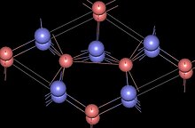
Tantalum nitride (TaN) is a chemical compound, a nitride of tantalum. There are multiple phases of compounds, stoichimetrically from Ta2N to Ta3N5, including TaN.
As a thin film TaN find use as a diffusion barrier and insulating layer between copper interconnects in the back end of line of computer chips. Tantalum nitrides are also used in thin film resistors.
Phase diagram
[edit]The tantalum - nitrogen system includes several states including a nitrogen solid solution in Tantalum, as well as several nitride phases, which can vary from expected stoichiometry due to lattice vacancies.[1] Annealing of nitrogen rich "TaN" can result in conversion to a two phase mixture of TaN and Ta5N6.[1]
Ta5N6 is thought to be the more thermally stable compound - though it decomposes in vacuum at 2500 °C to Ta2N.[1] It was reported the decomposition in vacuum from Ta3N5 via Ta4N5, Ta5N6, ε-TaN, to Ta2N.[2]
Preparation
[edit]TaN is often prepared as thin films. Methods of depositing the films include RF-magnetron-reactive sputtering,[3][4] Direct current (DC) sputtering,[5] Self-propagating high-temperature synthesis (SHS) via 'combustion' of tantalum powder in nitrogen,[1] low‐pressure metalorganic chemical vapor deposition (LP‐MOCVD),[6] ion beam assisted deposition (IBAD),[7] and by electron beam evaporation of tantalum in concert with high energy nitrogen ions.[8]
Depending on the relative amount of N2, the deposited film can vary from (fcc) TaN to (hexagonal) Ta2N as nitrogen decreases.[4] A variety of other phases have also been reported from deposition including bcc and hexagonal TaN; hexagonal Ta5N6; tetragonal Ta4N5; orthorhombic Ta6N2.5, Ta4N, or Ta3N5.[4] The electrical properties of TaN films vary from metallic conductor to insulator depending on the relative nitrogen ratio, with N rich films being more resistive.[9]
Uses
[edit]It is sometimes used in integrated circuit manufacture to create a diffusion barrier or "glue" layers between copper, or other conductive metals. In the case of BEOL processing (at c. 20 nm), copper is first coated with tantalum, then with TaN using physical vapour deposition (PVD); this barrier coated copper is then coated with more copper by PVD, and infilled with electrolytically coated copper, before being mechanically processed (grind/polishing).[10]
It also has application in thin film resistors.[3] It has the advantage over nichrome resistors of forming a passivating oxide film which is resistant to moisture.[11]
References
[edit]- ^ a b c d Borovinskaya, Inna P. (2017). "Tantalum Nitride". Concise Encyclopedia of Self-Propagating High-Temperature Synthesis - History, Theory, Technology, and Products. pp. 370–371. doi:10.1016/B978-0-12-804173-4.00150-2. ISBN 9780128041734.
- ^ Terao, Nobuzo (1971), "Structure of Tantalum Nitrides", Japanese Journal of Applied Physics, 10 (2): 248–259, Bibcode:1971JaJAP..10..248T, doi:10.1143/JJAP.10.248, S2CID 122356023
- ^ a b Akashi, Teruhisa (2005), "Fabrication of a Tantalum-Nitride Thin-Film Resistor with a Low-Variability Resistance", IEEJ Transactions on Sensors and Micromachines, 125 (4): 182–187, Bibcode:2005IJTSM.125..182A, doi:10.1541/ieejsmas.125.182
- ^ a b c Zaman, Anna; Meletis, Efstathios I. (23 November 2017), "Microstructure and Mechanical Properties of TaN Thin Films Prepared by Reactive Magnetron Sputtering", Coatings, 7 (12): 209, doi:10.3390/coatings7120209
- ^ Lima, Lucas; Moreiraa, Milena D.; Cioldin, Fred; Diniza, José Alexandre; Doi, Ioshiaki (2010), "Tantalum Nitride as Promising Gate Electrode for MOS Technology", ECS Trans., 31 (1): 319–325, Bibcode:2010ECSTr..31a.319L, doi:10.1149/1.3474175, S2CID 97901262
- ^ Tsai, M. H.; Sun, S. C. (1995), "Metalorganic chemical vapor deposition of tantalum nitride by tertbutylimidotris(diethylamido)tantalum for advanced metallization", Appl. Phys. Lett., 67 (8): 1128, Bibcode:1995ApPhL..67.1128T, doi:10.1063/1.114983
- ^ Baba, K.; Hatada, R.; Udoh, K.; Yasuda, K. (2 May 1997), "Structure and properties of NbN and TaN films prepared by ion beam assisted deposition", Nuclear Instruments and Methods in Physics Research Section B: Beam Interactions with Materials and Atoms, 127–128: 841–845, Bibcode:1997NIMPB.127..841B, doi:10.1016/S0168-583X(97)00018-9
- ^ Ensinger, W.; Kiuchi, M.; Satou, M. (1995), "Low-temperature formation of metastable cubic tantalum nitride by metal condensation under ion irradiation", Journal of Applied Physics, 77 (12): 6630, Bibcode:1995JAP....77.6630E, doi:10.1063/1.359073
- ^ Kim, Deok-kee; Lee, Heon; Kim, Donghwan; Kim, Young Keun (October 2005), "Electrical and mechanical properties of tantalum nitride thin films deposited by reactive sputtering", Journal of Crystal Growth, 283 (3–4): 404–408, Bibcode:2005JCrGr.283..404K, doi:10.1016/j.jcrysgro.2005.06.017
- ^ LaPedus, Mark (26 June 2012), "Challenges Mount For Interconnect", semiengineering.com
- ^ Licari, James J.; Enlow, Leonard R. (1998), Hybrid Microcircuit technology Handbook (2nd ed.), Noyes Publications, § 2.5 Characteristics of Tantalum Nitride Resistors, pp.83-4
