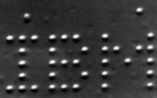
IBM (atoms)

IBM in atoms was a demonstration by IBM scientists in 1989 of a technology capable of manipulating individual atoms.[1] A scanning tunneling microscope was used to arrange 35 individual xenon atoms on a substrate of chilled crystal of nickel to spell out the three letter company initialism. It was the first time that atoms had been precisely positioned on a flat surface.[2][3]
Research
Donald Eigler and Erhard Schweizer of the IBM Almaden Research Center in San Jose, California, discovered the ability using a scanning tunneling microscope (STM) to move atoms about the surface.[4] In the demonstration, where the microscope was used in low temperature,[5] they positioned 35 individual xenon atoms on a substrate of chilled crystal of nickel to form the acronym "IBM".[1] The pattern they created was 5 nm tall and 17 nm wide. They also assembled chains of xenon atoms similar in form to molecules.[1] The demonstrated capacity showed the potential of fabricating rudimentary structures and allowed insights as to the extent of device miniaturization.[5]
See also
- There's Plenty of Room at the Bottom – Lecture by Richard Feynman
- A Boy and His Atom – The world's smallest movie
References
- ^ a b c Eigler, D. M.; Schweizer, E. K. (1990). "Positioning single atoms with a scanning tunnelling microscope". Nature. 344 (6266): 524–526. doi:10.1038/344524a0. ISSN 0028-0836.
- ^ "2 Researchers Spell 'I.B.M.,' Atom by Atom". The New York Times. 5 April 1990.
- ^ "IBM's 35 atoms and the rise of nanotech". CNET News.
- ^ Hey, Anthony J. G.; Hey, Tony; Walters, Patrick (2003). The New Quantum Universe. Cambridge, UK: Cambridge University Press. p. 82. ISBN 0521564182.
- ^ a b Baird, Davis; Nordmann, Alfred; Schummer, Joachim (2004). Discovering the Nanoscale. Amsterdam: IOS Press. pp. 140. ISBN 1586034677.
External links

