Latte (graphics chip)
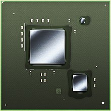
 An illustration of the Wii U MCM without heat spreader. The largest chip is the "Latte" GPU co-designed by AMD and Nintendo and manufactured by TSMC. The other chips are the "Espresso" CPU (smaller chip) from IBM and an unknown chip (tiny) from Renesas. | |
| General information | |
|---|---|
| Launched | 2012 |
| Discontinued | Present |
| Designed by | AMD and Nintendo |
| Common manufacturer | |
| Performance | |
| Max. CPU clock rate | 550 MHz[1][2] |
| Architecture and classification | |
| Application | Wii U |
| Technology node | 40 nm |
| History | |
| Predecessor | Hollywood |
Latte is the codename of the Graphics Processing Unit (GPU) and I/O chip used in Nintendo's Wii U video game console.[3] It was designed by Nintendo and AMD, and is currently being produced using a 40 nm advanced CMOS process. The Latte chip resides together with a CPU from IBM on a MCM manufactured by Renesas. It was revealed at E3 2011 in June 2011 and released in November 2012.
Design

AMD and Nintendo have revealed that the Latte graphics chip is based on the "Radeon HD" series of GPUs. Although there have been several reports of the GPU being based on the R700 family of AMD GPUs, die shots reveal a completely customized design which resembles no existing GPU on the market today. It is the largest die on the Wii U's MCM. The chip contains an Audio DSP, eDRAM, components for Wii Backward Compatibility,
Specifications
This section needs expansion. You can help by adding to it. (March 2013) |
- 3 Separate Blocks of memory:
- 1 Block of 32MB of eDRAM,
- 1 Block of 1MB of SRAM - Possibly used in "Wii mode",
- 1 Block of 2MB of eDRAM[4]
- Stream processing units (SPU): 320 clocked at 549.9 MHz
- ROP's: 8
- Texture mapping units: 16
Comparable to a heavily modified Radeon HD 4670/4650 albeit with less texture-mapping units.[5][6]
References
- ^ Leadbetter, Richard (29 November 2012). "Wii U has 1.24GHz CPU, 550MHz graphics core - report". Retrieved 8 February 2013.
- ^ Shilov, Anton (29 November 2012). "Detailed Specifications of Nintendo Wii U Revealed by Technology Enthusiasts". Retrieved 8 February 2013.
- ^ rwilliamson (February 4, 2013). "Looking at the Wii U Graphics Processor". http://www.chipworks.com. Retrieved 8 February 2013.
{{cite web}}: External link in|publisher= - ^ http://www.neogaf.com/forum/showthread.php?t=511628
- ^ http://www.neogaf.com/forum/showthread.php?t=511741
- ^ Here is a Forum Article on the matter: "http://www.eurogamer.net/articles/df-hardware-wii-u-graphics-power-finally-revealed"
