SuperH
| Designer | Hitachi Ltd. |
|---|---|
| Bits | 32-bit (32 → 64) |
| Introduced | 1990s |
| Design | RISC |
| Encoding | Fixed |
| Endianness | Bi |
SuperH (or SH) is a 32-bit reduced instruction set computing (RISC) instruction set architecture (ISA) developed by Hitachi and currently produced by Renesas. It is implemented by microcontrollers and microprocessors for embedded systems.
As of 2015[update], many of the original patents for the SuperH architecture are expiring and the SH2 CPU has been reimplemented as open source hardware under the name J2.
History

The SuperH processor core family was first developed by Hitachi in the early 1990s. Hitachi has developed a complete group of upward compatible instruction set CPU cores. The SH-1 and the SH-2 were used in the Sega Saturn and Sega 32X. These cores have 16-bit instructions for better code density than 32-bit instructions, which was a great benefit at the time, due to the high cost of main memory.
A few years later the SH-3 core was added to the SH CPU family; new features included another interrupt concept, a memory management unit (MMU) and a modified cache concept. The SH-3 core also got a DSP extension, then called SH-3-DSP. With extended data paths for efficient DSP processing, special accumulators and a dedicated MAC-type DSP engine, this core was unifying the DSP and the RISC processor world. A derivative was also used with the original SH-2 core.
Between 1994 and 1996, 35.1 million SuperH devices were shipped worldwide.[1]
For the Dreamcast, Hitachi developed the SH-4 architecture. Superscalar (2-way) instruction execution and a vector floating point unit (particularly suited to 3d graphics) were the highlights of this architecture. SH-4 based standard chips were introduced around 1998.
The SH-3 and SH-4 architectures support both big-endian and little-endian byte ordering (they are bi-endian).
Licensing
Hitachi and STMicroelectronics started collaborating as early as 1997 on the design of the SH-4. In early 2001, they formed the IP company SuperH, Inc., which was going to license the SH-4 core to other companies and was developing the SH-5 architecture, the first move of SuperH into the 64-bit area.[2][3] In 2003, Hitachi and Mitsubishi Electric formed a joint-venture called Renesas Technology, with Hitachi controlling 55% of it. In 2004, Renesas Technology bought STMicroelectronics's share of ownership in the SuperH Inc. and with it the licence to the SH cores.[4] Renesas Technology later became Renesas Electronics, following their merger with NEC Electronics.
The SH-5 design supported two modes of operation. SHcompact mode is equivalent to the user-mode instructions of the SH-4 instruction set. SHmedia mode is very different, using 32-bit instructions with sixty-four 64-bit integer registers and SIMD instructions. In SHmedia mode the destination of a branch (jump) is loaded into a branch register separately from the actual branch instruction. This allows the processor to prefetch instructions for a branch without having to snoop the instruction stream. The combination of a compact 16-bit instruction encoding with a more powerful 32-bit instruction encoding is not unique to SH-5; ARM processors have a 16-bit Thumb mode (ARM licensed several patents from SuperH for Thumb[5]) and MIPS processors have a MIPS-16 mode. However, SH-5 differs because its backward compatibility mode is the 16-bit encoding rather than the 32-bit encoding.
The evolution of the SuperH architecture still continues. The latest evolutionary step happened around 2003 where the cores from SH-2 up to SH-4 were getting unified into a superscalar SH-X core which forms a kind of instruction set superset of the previous architectures.
Today, the SuperH CPU cores, architecture and products are with Renesas Electronics, a merger of the Hitachi and Mitsubishi semiconductor groups and the architecture is consolidated around the SH-2, SH-2A, SH-3, SH-4 and SH-4A platforms giving a scalable family.
J Core
The last of the SH-2 patents expired in 2014. At LinuxCon Japan 2015, j-core developers presented a cleanroom reimplemention of the of the SH-2 ISA with extensions (known as the "J2 core" due to the unexpired trademarks).[5][6] Subsequently, a design walkthrough was presented at ELC 2016.[7]
The open source BSD licensed VHDL code for the J2 core has been proven on Xilinx FPGAs and on ASICs manufactured on TSMC's 180 nm process, and is capable of booting uClinux.[5] J2 is backwards ISA compatible with SH-2, implemented as a 5 stage pipeline with separate Instruction and Data memory interfaces, and a machine generated Instruction Decoder supporting the densely packed and complex (relative to other RISC machines) ISA. Additional instructions are easy to add. J2 implements instructions for dynamic shift (using the SH-3 and later instruction patterns), extended atomic operations (used for threading primitives) and locking/interfaces for symmetric multiprocessor support. Plans to implement the SH2A (as "J2+") and SH4 (as "J4") instruction sets as the relevant patents expire in 2016-2017.[5]
Several features of SuperH have been cited as motivations for designing new cores based on this architecture:[5]
- High code density compared to other 32-bit RISC ISAs such as ARM or MIPS[8] important for cache and memory bandwidth performance
- Existing compiler and operating system support (Linux, Windows Embedded, QNX[6])
- Extremely low ASIC fabrication costs now that the patents are expiring (around US$0.03 for a J2 dual core core on TSMC's 180 nm process).
- Patent and royalty free (BSD licensed) implementation
- Full and vibrant community support
- Availability of low cost hardware development platform for zero cost FPGA tools
- CPU and SoC RTL generation and integration tools, producing FPGA and ASIC portable RTL and documentation
- Clean, modern design with open source design, generation, simulation and verification environment
Models

The family of SuperH CPU cores includes:
- SH-1 - used in microcontrollers for deeply embedded applications (CD-ROM drives, major appliances, etc.)
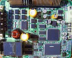
- SH-2 - used in microcontrollers with higher performance requirements, also used in automotive such as engine control units or in networking applications, and also in video game consoles, like the Sega Saturn. The SH-2 has also found home in many motor control applications, including Subaru, Mitsubishi, and Mazda.
- SH-2A - The SH-2A core is an extension of the SH-2 core including a few extra instructions but most importantly moving to a superscalar architecture (it is capable of executing more than one instruction in a single cycle) and two five-stage pipelines. It also incorporates 15 register banks to facilitate an interrupt latency of 6 clock cycles. It is also strong in motor control application but also in multimedia, car audio, powertrain, automotive body control and office + building automation
- SH-DSP - initially developed for the mobile phone market, used later in many consumer applications requiring DSP performance for JPEG compression etc.
- SH-3 - used for mobile and handheld applications such as the Jornada, strong in Windows CE applications and market for many years in the car navigation market
- SH-3-DSP - used mainly in multimedia terminals and networking applications, also in printers and fax machines
- SH-4 - used whenever high performance is required such as car multimedia terminals, video game consoles, or set-top boxes
- SH-5 - used in high-end 64-bit multimedia applications
- SH-X - mainstream core used in various flavours (with/without DSP or FPU unit) in engine control unit, car multimedia equipment, set-top boxes or mobile phones
- SH-Mobile - SuperH Mobile Application Processor; designed to offload application processing from the baseband LSI
SH-2

The SH-2 is a 32-bit RISC architecture with a 16-bit fixed instruction length for high code density and features a hardware multiply–accumulate (MAC) block for DSP algorithms and has a five-stage pipeline.
The SH-2 has a cache on all ROM-less devices.
It provides 16 general purpose registers, a vector-base-register, global-base-register, and a procedure register.
Today the SH-2 family stretches from 32 KB of on-board flash up to ROM-less devices. It is used in a variety of different devices with differing peripherals such as CAN, Ethernet, motor-control timer unit, fast ADC and others.
SH-2A
The SH-2A is an upgrade to the SH-2 core. It was announced in early 2006.
At launch in 2007 the SH-2A based SH7211 was the world's fastest embedded flash microcontroller running at 160 MHz. It has later been superseded by several newer SuperH devices running at up to 200 MHz.
New features on the SH-2A core include:
- Superscalar architecture: execution of 2 instructions simultaneously
- Harvard architecture
- Two 5-stage pipelines
- 15 register banks for interrupt response in 6 cycles.
- Optional FPU
The SH-2A family today spans a wide memory field from 16 KB up to and includes many ROM-less variations. The devices feature standard peripherals such as CAN, Ethernet, USB and more as well as more application specific peripherals such as motor control timers, TFT controllers and peripherals dedicated to automotive powertrain applications.
SH-4

The SH-4 is a 32-bit RISC CPU and was developed for primary use in multimedia applications, such as Sega's Dreamcast and NAOMI game systems. It includes a much more powerful floating point unit and additional built-in functions, along with the standard 32-bit integer processing and 16-bit instruction size.
SH-4 features include:
- FPU with four floating point multipliers, supporting 32-bit single precision and 64-bit double precision floats
- 4D floating point dot-product operation
- 128-bit floating point bus allowing 3.2 GB/sec transfer rate from the data cache
- 64-bit external data bus with 32-bit memory addressing, allowing a maximum of 4 GB addressable memory with a transfer rate of 800 MB/sec
- Built-in interrupt, DMA, and power management controllers
SH-5
The SH-5 is a 64-bit RISC CPU.[citation needed]
Almost no non-simulated SH-5 hardware was ever released,[9] and unlike the still live SH-4, support for SH-5 is being dropped from gcc.[10]
References
- ^ http://segatech.com/technical/cpu/tech_sh4.html
- ^ "STMicro, Hitachi plan new company to develop RISC cores". EE Times. 3 April 2001.
Hitachi created the SH family of processors and developed its first four major iterations, but has worked with ST since 1997, when the companies agreed to share a common high-end microprocessor road map. They jointly developed the 32-bit SH4 RISC processor core, and began development of the SH5 architecture, which will now be completed by SuperH. SuperH's initial product will be the SH4 core. Earlier SH versions will not be part of the spin-off agreement.
- ^ "SuperH, Inc. formed by Hitachi and STMicroelectronics to Boost the Proliferation of SuperH™ Cores in Embedded Microprocessor Applications".
- ^ "Renesas to take over SuperH core business". EE Times. 28 September 2004.
- ^ a b c d e Nathan Willis (June 10, 2015). "Resurrecting the SuperH architecture". LWN.net.
- ^ a b "J Cores". j-core. Retrieved April 27, 2016.
- ^ http://j-core.org/talks/ELC-2016.pdf
- ^ V.M. Weaver (17 March 2015). "Exploring the Limits of Code Density (Tech Report with Newest Results)" (PDF).
- ^ "Wasabi SH-5 Press Release". 8 March 2016.
- ^ "GCC 6 Release Series -- Changes, New Features, and Fixes". 31 January 2016.
