Pentium (original)
 The Intel Pentium family | |
| General information | |
|---|---|
| Launched | 1993 |
| Discontinued | 1999 |
| Common manufacturer |
|
| Performance | |
| Max. CPU clock rate | 60 MHz to 300 MHz |
| FSB speeds | 50 MHz to 66 MHz |
| Architecture and classification | |
| Technology node | 0.8µm to 0.25µm |
| Microarchitecture | P5 |
| Instruction set | x86 |
| Physical specifications | |
| Cores |
|
| Socket |
|
| Products, models, variants | |
| Core name |
|
The P5 microarchitecture is the implementation of the original Intel Pentium microprocessor, which was introduced on March 22, 1993 as the first superscalar x86 processor.[1][2] The microarchitecture was a direct extension of the 80486 architecture and included dual integer pipelines, a faster FPU, wider data bus, separate code and data caches and features for further reduced address calculation latency. In 1996, the Pentium MMX was introduced with the same basic microarchitecture complemented with MMX instructions, larger caches, and some other enhancements.
The name Pentium was derived from the Greek pente (πέντε), meaning 'five', and the Latin ending -ium, a name selected after courts had disallowed trademarking of number-based names like "i586" or "80586". Intel filed a U.S. trademark for the name 'Pentium' on July 2, 1992, more than 8 months before the public release of the Intel Pentium chip with the description 'computer hardware; namely, microprocessors'.[3] In 1995, Intel started to employ the registered Pentium trademark also for x86 processors with radically different microarchitectures (Pentium Pro / II / III / 4 / D / M). In 2006, the Pentium brand briefly disappeared from Intel's roadmaps,[4][5] only to re-emerge in 2007.[6]
Vinod Dham is often referred to as the father of the Intel Pentium processor,[7][8] although many people, including John H. Crawford (of i386 and i486 alumni), were involved in the design and development of the processor.
Improvements over i486
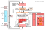
- Superscalar architecture — The Pentium has two datapaths (pipelines) that allow it to complete more than one instruction per clock cycle. One pipe (called U) can handle any instruction, while the other (called V) can handle the simplest, most common instructions. Some RISC proponents had argued that the "complicated" x86 instruction set would probably never be implemented by a tightly pipelined microarchitecture, much less by a dual pipeline design. The 486 and the Pentium demonstrated that this was indeed possible and feasible.
- 64-bit external databus width — This doubles the amount of information read or written on each memory access. This doesn't mean that the Pentium can execute 64-bit applications; its main registers are still 32 bits wide.
- Faster floating point unit.
- MMX instructions (later models only) - A basic SIMD instruction set extension designed for use in multimedia applications.
- Virtualized interrupt to speed up virtual 8086 mode.
- Enhanced debug features with the introduction of the Processor-based debug port (See Pentium Processor Debugging in the Developers Manual, Vol 1).
- Enhanced self test features like the L1 cache parity check (see Cache Structure in the Developers Manual, Vol 1).
Pentium architecture chips offered just under twice the performance of a 486 processor per clock cycle. The fastest Intel 486 parts were almost as powerful as a first-generation Pentium, and the AMD Am5x86 was roughly equal to the Pentium 75.
The Pentium ("Classic") series were designed to run at over 100 million instructions per second (MIPS),[9] with the 75 MHz model running at 126.5 MIPS.[10]
Models
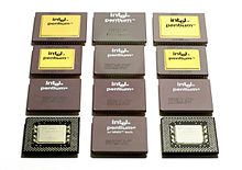
The Pentium was Intel's primary microprocessor for personal computers during the mid-1990s. The original design was reimplemented in newer processes and new features were added to maintain its competitiveness as well as to address specific markets such as portable computers. As a result, there were six variants of the Pentium.
P5

The original Pentium microprocessor was code-named "P5". Its product code was 80501 (80500 for the earliest steppings) and it operated at 60 MHz and 66 MHz. It contained 3.1 million transistors and measured 16.7 mm by 17.6 mm for an area of 293.92 mm2.[11] It was fabricated in a 0.8 µm BiCMOS process.
P54C
The P5 was followed by the P54C (80502), which operated at 75, 90 and 100 MHz. It employed an internal clock multiplier to let the internal circuitry work at a higher frequency than the front side bus, as it is much more difficult to increase the front side bus frequency. It also allowed two-way multiprocessing. It contained 3.3 million transistors and measured 163 mm2.[12] It was fabricated in a 0.5 µm (described by Intel as "0.6 µm") BiCMOS process.[12]
P54CQS
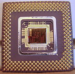
The P54C was followed by the P54CQS which operated at 120 MHz. It was fabricated in a 0.35 µm BiCMOS process, unlike early rumors of it being a CMOS design, and was the first commercial microprocessor to be fabricated in a 0.35 µm process.[12] It had an identical transistor count to the P54C and despite the newer process, it had an identical area as well. The reason for this was because of time-to-market requirements. The chip was connected to the package using wire bonding, which only allows connections along the edges of the chip. A smaller chip would have required a redesign of the package, as there is a limit on the length of the wires and the edges of the chip would be further away from the pads on the package. The solution was to keep the chip at the same size, retain the existing pad-ring, and only reduce the size of the Pentium's logic circuitry to enable it to achieve higher clock frequencies.[12]
P54CS
The P54CQS was followed by the P54CS, which operated at 133, 150, 166 and 200 MHz. It contained 3.3 million transistors, measured 90 mm2 and was fabricated in a 0.35 µm BiCMOS process with four levels of interconnect.
Bugs and problems
The early versions of 60-100 MHz Pentiums had a problem in the floating point unit that resulted in incorrect (but predictable) results from some division operations. This bug, discovered in 1994 by professor Thomas Nicely at Lynchburg College, Virginia, became known as the Pentium FDIV bug and caused embarrassment for Intel, which created an exchange program to replace the faulty processors. Soon afterwards, a bug was discovered which could allow a malicious program to crash a system without any special privileges (the f00f bug); fortunately, operating systems were able to implement workarounds to prevent crashes.
The 60 and 66 MHz 0.8 µm versions of the Pentium processors also had (for the time) high heat production due to their 5V operation, and were often known colloquially as "coffee warmers" or some similar nickname.[citation needed] The P54C used 3.3V and had significantly lower power draw (a quadratic relationship). P5 Pentiums used Socket 4, while P54C started out on Socket 5 before moving to Socket 7 in later revisions. All desktop Pentiums from P54CS onwards used Socket 7.
Pentium OverDrive
The P24T Pentium OverDrive for 486-systems were released in 1995, which were based on 3.3V 0.6 µm versions using a 63 or 83 MHz clock. Since these used Socket 2/3, some modifications had to be made to compensate for the 32-bit data bus and slower on-board L2 cache of 486-motherboards. They were therefore equipped with a 32KB L1 cache (double that of pre-P55C Pentiums).
P55C, Tillamook


The P55C (or 80503) was developed by Intel's Research & Development Center in Haifa, Israel. It was sold as Pentium with MMX Technology (usually just called Pentium MMX); although it was based on the P5 core it featured a new set of 57 "MMX" instructions intended to improve performance on multimedia tasks, such as encoding and decoding digital media data. The Pentium MMX line was introduced on 22 October 1996.[13]
The new instructions work on new data types: 64-bit packed vectors of either eight 8-bit integers, four 16-bit integers, two 32-bit integers, or one 64-bit integer. So, for example, the PADDUSB (Packed ADD Unsigned Saturated Byte) instruction adds two vectors, each containing eight 8-bit unsigned integers together, pairwise; each addition that would overflow saturates, yielding 255, the maximum unsigned value that can be represented in a byte. These rather specialized instructions generally require special coding by the programmer for them to be used. The performance of the P55C was improved over previous versions by a doubling of the Level 1 CPU cache from 16 KB to 32 KB.
It contained 4.5 million transistors and had an area of 140 mm2. It was fabricated in a 0.28 µm CMOS process with the same metal pitches as the previous 0.35 µm BiCMOS process, so Intel described it as "0.35 µm" because of its similar transistor density.[14] The process has four levels of interconnect.[14]
Pentium P55C notebook CPUs used a "mobile module" that held the CPU. This module was a PCB with the CPU directly attached to it in a special smaller form factor. The module snapped to the notebook motherboard and typically a heat spreader plate was installed and made contact with the module. Such notebooks frequently used the Intel 430MX chipset, a feature-reduced 430FX. However, with the 0.25 µm Tillamook Mobile Pentium MMX (named after a city in Oregon), the module also held the 430TX chipset along with the system's 512 KB SRAM cache memory.
While the P55C is compatible with the common Socket 7 motherboard configuration, the voltage requirements for powering the chip differ from the standard Socket 7 specifications. Due to certain manufacturers not preparing for the introduction of MMX technology most motherboards manufactured for Socket 7 previous to the establishment of the P55C standard are not compliant with the dual intensity required for proper operation of this chip. The Intel Corporation temporarily manufactured a conversion kit called the Overdrive that was designed to correct this lack of planning on the motherboard manufacturers part.
Models and variants

|

|
 |

|
 |

|
 |
 |
 | ||||||||||||
| Code name | P5 | P54C | P54CS | P55C | Tillamook | |||||||||||||||
| Product code | 80500/ 80501 | 80502 | 80503 | |||||||||||||||||
| Process size (µm) | 0.80 | 0.60 or 0.35* | 0.35 | 0.35 (later 0.28) | 0.25 | |||||||||||||||
| Socket | Socket 4 | Socket 5/7 | Socket 7 | |||||||||||||||||
| Package | CPGA | CPGA/TCP* | CPGA/PPGA/TCP* | CPGA/PPGA/TCP* | TCP/TCP on MMC-1 | |||||||||||||||
| Clock speed (MHz) | 60 | 66 | 75 | 90 | 100 | 120 | 133 | 150 | 166 | 200 | 120* | 133* | 150* | 166 | 200 | 233 | 200 | 233 | 266 | 300 |
| Bus speed (MHz) | 60 | 66 | 50 | 60 | 66 | 60 | 66 | 60 | 66 | 60 | 66 | 60 | 66 | |||||||
| Voltage | 5.0 | 5.0 | 3.3 2,9* | 3.3 2.9* | 3.3 3.1* 2.9* | 3.3 3.1* 2.9* | 3.3 3.1* 2.9* | 3.3 3.1* 2.9* | 3.3 | 3.3 | 2.8 | 2.45 | 2.45 | 2.8 | 2.8 | 2.8 | 1.8 | 1.8 | 1.8 | 1.8 |
| Introduced | 1993-03-22 | 1994-10-10 | 1994-03-07 | 1995-03-27 | 1995-06 | 1996-01-04 | 1996-06-10 | 1995-03-27 - 1995-11-01 | 1997-01-08 | 1997-06-02 | 1997-08 | 1998-01 | 1999-01 | |||||||
| An asterisk indicates that these were only available as Mobile Pentium or Mobile Pentium MMX chips for laptops. | ||||||||||||||||||||
 | |||||||
| Code name | P54CTB | ||||||
| Product code | PODPMT60X150 | PODPMT66X166 | PODPMT60X180 | PODPMT66X200 | |||
| Process size (µm) | 0.35 | ||||||
| Socket | Socket 5/7 | ||||||
| Package | CPGA with heatsink, fan and voltage regulator | ||||||
| Clock speed (MHz) | 125 | 150 | 166 | 150 | 180 | 200 | |
| Bus speed (MHz) | 50 | 60 | 66 | 50 | 60 | 66 | |
| Upgrade for | Pentium 75 | Pentium 90 | Pentium 100 and 133 | Pentium 75 | Pentium Pentium 90, 120 and 150 | Pentium 100, 133 and 166 | |
| TDP (max. W) | 15,6 | 15,6 | 15,6 | 18 | |||
| Voltage | 3,3 | 3,3 | 3,3 | 3,3 | |||
 |
 | ||||||
| Code name | P55C | Tillamook | |||||
| Product code | FV8050366200 | FV8050366233 | FV80503CSM66166 | GC80503CSM66166 | GC80503CS166EXT | FV80503CSM66266 | GC80503CSM66266 |
| Process size (µm) | 0.35 | 0.25 | |||||
| Clock speed (MHz) | 200 | 233 | 166 | 166 | 166 | 266 | 266 |
| Bus speed (MHz) | 66 | 66 | 66 | 66 | 66 | 66 | 66 |
| Package | PPGA | PPGA | PPGA | BGA | BGA | PPGA | BGA |
| TDP (max. W) | 15,7 | 17 | 4.5 | 4.1 | 4.1 | 7.6 | 7.6 |
| Voltage | 2.8 | 2.8 | 1.9 | 1.8 | 1.8 | 1.9 | 2.0 |
See also
- CPU design
- COASt (Cache On A Stick), L2 cache modules for Pentium
- IA-32 instruction set architecture (ISA)
- Pentium compatible processor
Competitors
References
- ^ "View Processors Chronologically by Date of Introduction:". Intel. Retrieved 2007-08-14.
- ^ "Intel Pentium Processor Family". Intel. Retrieved 2007-08-14.
- ^ http://www.trademarkia.com/pentium-74291248.html
- ^ "Intel "Conroe-L" Details Unveiled". DailyTech. Retrieved 2007-08-16.
- ^ The multicore era is upon us - CNET Asia
- ^ "Intel to unify product naming scheme". TG Daily. Retrieved 2007-08-12.
- ^ "Vinod Dham, Father of Pentium Processor, on Investing in India". PodTech.net. 2006-10-16. Retrieved 2007-08-16.
Vinod Dham, Father of Pentium Processor
- ^ Bach, John (2000). "The Technology Trailblazer: Vinod Dham". University Relations, University of Cincinnati. Retrieved 2007-08-16.
Today, known in the industry as the Father of the Pentium
{{cite web}}: Unknown parameter|month=ignored (help) - ^ http://dede.essortment.com/pcusersguides_rjje.htm
- ^ http://www.islandnet.com/~kpolsson/micropro/proc1994.htm
- ^ Case, Brian (29 March 1993). "Intel Reveals Pentium Implementation Details". Microprocessor Report.
- ^ a b c d Gwennap, Linley (27 March 1995). "Pentium is First CPU to Reach 0.35 Micron". Microprocessor Report.
- ^ "New Chip Begs New Questions". CNet. Retrieved 2009-02-06.
- ^ a b Slater, Michael (5 March 1996). "Intel's Long-Awaited P55C Disclosed". Microprocessor Report.
External links
- CPU-Collection.de - Intel Pentium images and descriptions
- Plasma Online Intel CPU Identification
- Pictures of all known Pentium chips at chipdb.org
- The Pentium Timeline Project The Pentium Timeline Project maps oldest and youngest chip known of every s-spec made. Data are shown in a interactive timeline.
Intel Datasheets
- Pentium (P5)
- Pentium (P54)
- Pentium MMX (P55C)
- Mobile Pentium MMX (P55C)
- Mobile Pentium MMX (Tillamook)
Intel Manuals
These Manuals do provide a overview of the Pentium Processor and its features:
- Pentium® Processor Family Developer’s Manual Pentium® Processor (Volume 1) (Intel Order Number 241428)
- Pentium® Processor Family Developer’s Manual Volume 2: Instruction Set Reference (Intel Order Number 243191)
- Pentium® Processor Family Developer’s Manual Volume 3: Architecture and Programming Manual (Intel Order Number 241430)
