
x87
x87 is a floating point related subset of the x86 architecture instruction set. The term derives from the originally separate floating point coprocessors that had names ending in "87". Like other extensions to the basic instruction set, these instructions are not strictly needed to construct working programs, but provide hardware and microcode implementations of common numerical tasks, allowing these tasks to be performed much faster than corresponding machine code routines can. The x87 instruction set includes instructions for basic floating point operations such as addition, subtraction and comparision, but also for more complex numerical operations, such as the computation of the tangent or arctangent of a value, for example.
Most x86 processors since the Intel 80486 have had these x87 instructions implemented in the main CPU but the term is sometimes still used to refer to that part of the instruction set. Before x87 instructions were standard in PCs, compilers or programmers had to use rather slow library calls to perform floating-point operations, a method that is still common in (low cost) embedded systems.
Description
The x87 family does not use a directly addressable register set such as the main registers of the x86 processors; instead the x87 registers form a 8-level deep stack structure ranging from ST(0) to ST(7). The x87 instructions typically operate by pushing, calculating, and popping values on this stack with monadic operations (FSQRT, FPTAN etc) implicitly addressing the topmost ST(0) and dyadic operations (FADD, FMUL, FCOM, etc) implicitly addressing ST(0) and ST(1). However, this model can be modified as dyadic operations may use ST(0) also together with a direct memory operand or with an explicitly specified stack-register, ST(x), in a role similar to a traditional accumulator (a combined destination and left operand). This can also be reversed (on an instruction by instruction basis) with ST(0) as an unmodified operand and ST(x) as the destination. Furthermore, the contents in ST(0) can be exchanged with another stack register using an instruction called FXCH ST(x). These properties makes the x87 stack useable as seven freely addressable registers plus a dedicated accumulator. This is especially appliciable on superscalar x86 processors (Pentium of 1993 and later) where these exchange instructions (codes D9C8..D9CFh) are optimized down to a zero clock penalty (by using one of the integer paths for FXCH ST(x) in parallel with the FPU instruction). Despite being natural and convenient for human assembly language programmers, some compiler writers have found it complicated to construct automatic code generators that schedule x87 code effectively.
The x87 instructions are compatible with the IEEE-754 standard for floating-point. However, since the x87 processors all uses 80-bit wide registers internally (to allow for sustained precision over many calculations), it does not perform roundings exactly as the strict 32-bit and 64-bit IEEE-754 formats do, unless a special rounding mode is configured via a special configuration/status register. A given sequence of arithmetic operations may thus behave slightly different compared to strict IEEE-754 formats dependent on these settings.[1] Since the introduction of SSE2, the x87 instructions are not as essential as they once was, except for high precision calculations demanding the 64-bit mantissa precision available in the 80-bit format.
Performance
Clock cycle counts for examples of typical x87 FPU instructions (only register-register versions shown here)[2].
The A~B notation (best case to worst case) covers timing variations dependent on transient pipeline status as well as the arithmetic precision chosen (32, 64 or 80 bits); it also includes variations due to numerical cases (such as the number of set bits, zero, etc). The L→H notation depicts values corresponding to the lowest (L) and the highest (H) maximum clock frequency that was available.
| x87 implementation | FADD | FMUL | FDIV | FXCH | FCOM | FSQRT | FPTAN | FPATAN | Max Clock | Peak FMUL/sec | This x87 / 8087§ FMUL speed |
|---|---|---|---|---|---|---|---|---|---|---|---|
| 8087 | 70~100 | 90~145 | 193~203 | 10~15 | 40~50 | 180~186 | 30~540 | 250~800 | 5→10 MHz | 34~55K → 100~111K | 1.0 → 2.0 times as fast |
| 80287 (original) | 70~100 | 90~145 | 193~203 | 10~15 | 40~50 | 180~186 | 30~540 | 250~800 | 6→12 MHz | 41~66K → 83~133K | 1.2 → 2.4 times as fast |
| 80387 (and later 287 models) | 23~34 | 29~57 | 88~91 | 18 | 24 | 122~129 | 191~497 | 314~487 | 16→33 MHz | 280~552K → 579~1100K | approx 10 → 20 times as fast |
| 80486 (or 80487) | 8~20 | 16 | 73 | 4 | 4 | 83~87 | 200~273 | 218~303 | 16→50 MHz | 1.0M → 3.1M | approx 18 → 56 times as fast |
| Cyrix 6x86, Cyrix MII | 4~7 | 4~6 | 24~34 | 2 | 4 | 59~60 | 117~129 | 97~161 | 66→300 MHz | 11~16M → 50~75M | approx 320 → 1400 × as fast |
| AMD K6 (including K6 II/III) | 2 | 2 | todo | 2 | todo | todo | todo | todo | 166→550 MHz | 83M → 275M | approx 1500 → 5000 × as fast |
| Pentium / Pentium MMX | 1~3 | 1~3 | 39 | 1 (0*) | 1~4 | 70 | 17~173 | 19~134 | 60→300 MHz | 20~60M → 100~300M | approx 1100 → 5400 × as fast |
| Pentium Pro | 1~3 | 2~5 | 16~56 | 1 (0*) | 1 | 28~68 | todo | todo | 150→200 MHz | 30~75M → 40~100M | approx 1400 → 1800 × as fast |
| Pentium II / III | 1~3 | 2~5 | 17~38 | 1 (0*) | 1 | 27~50 | todo | todo | 233→1400 MHz | 47~116M → 280~700M | approx 2100 → 13000 × as fast |
| Athlon (K7) | 1~4 | 1~4 | 13~24 | 1 (0*) | 1~2 | 16~35 | todo | todo | 500→2330 MHz | 125~500M → 0.580~2.33G | approx 9000 → 58000 × as fast |
| Pentium 4 | 1~5 | 2~7 | 20~43 | 1 (0*) | todo | 20~43 | todo | todo | 1.3→3.8 GHz | 186~650M → 0.543~1.90G | approx 11000 → 34000 × as fast |
| Athlon 64 (K8) | 1~4 | 1~4 | 13~24 | 1 (0*) | 1~2 | 16~35 | todo | todo | 1.0→3.2 GHz | 250~1000M → 0.800~3.2G | approx 18000 → 58000 × as fast |
* An effective zero clock delay is often possible, via superscalar execution.
§ Compared to an original 5 MHz 8087. Using software-implemented floating point (a 8086 without a 8087), the factors would be significantly larger (perhaps another factor of 10).
Manufacturers
Companies that has designed and/or manufactured floating point units compatible with the Intel 8087 or later models include AMD (287, 387, 486DX, 5x86, K5, K6, K7, K8), Chips and Technologies (the Super MATH coprocessors), Cyrix (the FasMath, Cx87SLC, Cx87DLC, etc, 6x86, Cyrix MII), Fujitsu (early Pentium Mobile etc), IBM (various 387 and 486 designs), IDT (the C3, C7, Nano, etc), IIT (the 2C87, 3C87, etc), LC Technology (the Green MATH coprocessors), National Semiconductor (the Geode GX1, Geode GXm, etc), NexGen (the Nx587), Rise Technology (the mP6), ST Microelectronics (manufactured 486DX, 5x86, etc), Texas Instruments (manufactured 486DX processors), Transmeta (the TM5600 and TM5800), ULSI (the Math·Co coprocessors), VIA (the C3, C7, and Nano, etc), and Xtend (the 83S87SX-25 and other coprocessors).
8087
The 8087 was the first math coprocessor for 16 bit processors designed by Intel (the I8231 was older but designed for the 8 bit Intel 8080); it was built to be paired with the Intel 8088 and 8086 microprocessors.
80287


The 80287 (i287) was the math coprocessor for the Intel 80286 series of microprocessors. Intel (and its competitors) later introduced an 80287XL, which was actually an 80387SX with a 287 pinout. The 80287XL contained an internal 3/2 multiplier so that motherboards which ran the coprocessor at 2/3 CPU speed could instead run the FPU at the same speed of the CPU. Other 287-models with 387-like performance were the Intel 80C287 built in CHMOS III and the AMD 80EC287 manufactured in AMDs CMOS process, using only fully static gates.
The 80287 and 80287XL also worked with the 80386 microprocessor, and was initially the only coprocessor available for the 80386 until the introduction of the 80387 in 1987. Finally, it was also able to work with the Cyrix Cx486SLC. However for both of these chips the 80387 was strongly preferred for performance reasons and the greater capability of the instruction set.
Models
- i80287-3 (6MHz)
- i80287-6 (6MHz)
- i80287-8 (8MHz)
- i80287-10 (10MHz)
- i80287-12 (12.5MHz)
- i80287XL (12.5MHz, 387SX core)
- i80287XLT (12.5MHz, laptop version)
80387
The 80387 (387 or i387) was the first Intel coprocessor to be fully compliant with the IEEE 754 standard. Released in 1987, a full two years after the 386 chip, the i387 included much improved speed over Intel's previous 8087/80287 coprocessors, and improved the characteristics of trigonometric functions. (The 80287 limited the argument range to plus or minus 45 degrees.)
Without a coprocessor, the 386 normally performed floating-point arithmetic through (slow) software routines, implemented at runtime through a software exception-handler. When a math coprocessor is paired with the 386, the coprocessor performs the floating point arithmetic in hardware, returning results much faster than an (emulated) software library call.
The i387 was compatible only with the standard i386 chip, which had a 32-bit processor bus. The later cost-reduced i386SX, which had a narrower 16-bit data bus, could not interface with the i387's 32-bit bus. The i386SX required its own coprocessor, the Intel 80387SX, which was compatible with the SX's narrower 16-bit data-bus.
-
 i387
i387 -
 i387DX
 -
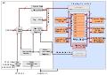 i387 microarchitecture with 16-bit Barrel shifter and CORDIC unit


80487

The i487 is a floating point unit coprocessor for Intel i486SX machines. It was essentially a full-blown i486DX chip. When installed into an i486SX system, the i487 disabled the main CPU and took over all CPU operations. In theory the computer would be able to operate if the original i486SX CPU was removed, although in practice a pin on the i487 prevented this.
References
- ^ David Monniaux, The pitfalls of verifying floating-point computations, to appear in ACM TOPLAS
- ^ Numbers are taken from respectice processors data sheets, programming manuals, and/or optimization manuals.
- Intel Corp., IA-32 Intel Architecture Software Developer's Manual Volume 1: Basic Architecture, order number 253665-017