Testing sandbox version[edit]
{{Infobox CPU/sandbox}}
MOS Technology 6502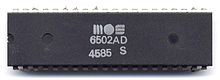 A MOS 6502 processor in a DIP-40 plastic package. The four-digit date code indicates it was made in the 45th week of 1985 | |
| Launched | 1975; 49 years ago (1975) |
|---|
| Common manufacturer(s) | |
|---|
|
| Max. CPU clock rate | 1 MHz to 2 MHz |
|---|
| Data width | 8 |
|---|
| Address width | 16 |
|---|
|
| Instruction set | MOS 6502 |
|---|
| Instructions | 56 |
|---|
|
| Package(s) | |
|---|
P6 | |
| Launched | November 1, 1995; 28 years ago (November 1, 1995) |
|---|
|
| Max. CPU clock rate | 150[5] MHz to 1.40 GHz |
|---|
| FSB speeds | 66 MHz to 133 MHz |
|---|
|
| L1 cache | Pentium Pro: 16 KB (8 KB I cache + 8 KB D cache)
Pentium II/III: 32 KB (16 KB I cache + 16 KB D cache) |
|---|
| L2 cache | 128 KB to 512 KB
256 KB to 2048 KB (Xeon) |
|---|
|
| Microarchitecture | P6 |
|---|
| Instruction set | x86 |
|---|
| Extensions | - MMX (Pentium II/III)
SSE (Pentium III)
|
|---|
|
| Transistors | |
|---|
| Cores | |
|---|
| Socket(s) | |
|---|
|
| Model(s) | - Celeron Series
- Pentium II Series
- Pentium III Series
- Pentium Pro Series
- Pentium II Xeon Series
- Pentium III Xeon Series
|
|---|
| Variant(s) | - Pentium M
- Enhanced Pentium M
|
|---|
|
| Predecessor | P5 |
|---|
| Successor | NetBurst, Pentium M |
|---|
|
| Unsupported |
NetBurst|
| Launched | November 20, 2000; 23 years ago (November 20, 2000) |
|---|
|
| Max. CPU clock rate | 1.3 GHz to 3.8 GHz |
|---|
| FSB speeds | 400 MT/s to 1066 MT/s |
|---|
|
| L1 cache | 8 KB to 16 KB per core |
|---|
| L2 cache | 128 KB to 2048 KB |
|---|
| L3 cache | 4 MB to 16 MB shared |
|---|
|
| Microarchitecture | NetBurst |
|---|
| Instruction set | x86 (IA-32), x86-64 (some) |
|---|
| Extensions | |
|---|
|
| Transistors | - 42M 180 nm (B2, C1, D0, E0)
- 55M 130 nm (B0, C1, D1, M0)
- 125M 90 nm (C0, D0, E0, G1)
- 169M 90 nm (M0, N0, R0)
- 230M 90 nm (A0, B0)
- 188M 65 nm (B1, C1, D0)
- 376M 65 nm (B1, C1, D0)
- 1,328M 65 nm (B0)
|
|---|
| Cores | - 1-2 (2-4 threads with HT)
|
|---|
| Socket(s) | |
|---|
|
| Model(s) | - Celeron Series
- Celeron D Series
- Pentium 4 Series
- Pentium D Series
- Xeon Series
|
|---|
|
| Predecessor | P6 |
|---|
| Successor | Intel Core
IA-64 |
|---|
Sandy Bridge|
| Launched | January 9, 2011; 13 years ago (January 9, 2011) |
|---|
| Discontinued | September 27, 2013 [6] |
|---|
| Product code | 80619 (extreme desktop)
80620 (server LGA1356)
80621 (server LGA2011)
80623 (desktop)
80627 (mobile) |
|---|
|
| Max. CPU clock rate | 1.60 GHz to 3.60 GHz |
|---|
| DMI speeds | 5.00 GT/s GT/s |
|---|
|
| L1 cache | 64 KB per core |
|---|
| L2 cache | 256 KB per core |
|---|
| L3 cache | 1 MB to 8 MB shared
10 MB to 15 MB (Extreme)
3 MB to 20 MB (Xeon) |
|---|
|
| Microarchitecture | Sandy Bridge |
|---|
| Instruction set | x86-64 |
|---|
| Instructions | x86, x86-64 |
|---|
| Extensions | - MMX, SSE, SSE2, SSE3, SSSE3, SSE4, SSE4.1, SSE4.2, AVX
- VT-x, VT-d
- AES-NI, CLMUL, TXT
|
|---|
|
| Transistors | |
|---|
| Cores | - 1–4 (4-6 Extreme, 2-8 Xeon)
|
|---|
| GPU(s) | HD Graphics
650 MHz to 1100 MHz
HD Graphics 2000
650 MHz to 1250 MHz
HD Graphics 3000
650 MHz to 1350 MHz
HD Graphics P3000
850 MHz to 1350 MHz |
|---|
| Socket(s) | |
|---|
|
| Model(s) | |
|---|
|
| Predecessor | Nehalem (Tock)
Westmere (Tick) |
|---|
| Successor | Ivy Bridge (Tick)
Haswell (Tock) |
|---|
|
| Unsupported |
Ivy Bridge Intel's internal Ivy Bridge logo [7] | |
| Launched | April 29, 2012; 12 years ago (April 29, 2012) |
|---|
| Discontinued | June 5, 2015; 8 years ago (June 5, 2015) |
|---|
| Marketed by | Intel |
|---|
| Designed by | Intel |
|---|
| Common manufacturer(s) | |
|---|
| CPUID code | 0306A9h |
|---|
| Product code | 80633 (extreme desktop)
80634 (server LGA1356)
80635 (server E5 LGA2011)
80636 (server E7 LGA2011)
80637 (desktop)
80638 (mobile) |
|---|
|
| Max. CPU clock rate | 1.4 to 4.1 GHz |
|---|
| DMI speeds | 5.00 GT/s |
|---|
|
| L1 cache | 64 KB per core |
|---|
| L2 cache | 256 KB per core |
|---|
| L3 cache | 2 to 8 MB shared |
|---|
|
| Technology node | Intel 22 nm |
|---|
| Microarchitecture | Sandy Bridge |
|---|
| Instruction set | x86-64 |
|---|
| Instructions | x86, x86-64 |
|---|
| Extensions | - MMX, SSE, SSE2, SSE3, SSSE3, SSE4, SSE4.1, SSE4.2, AVX, F16C
- AES-NI, CLMUL, RDRAND, TXT
- VT-x, VT-d
|
|---|
|
| Transistors | |
|---|
| Cores | - 2–4 (Mainstream)
2–15 (Xeon)
|
|---|
| GPU(s) | HD Graphics 2500
650 to 1150 MHz
HD Graphics 4000
350 to 1300 MHz
HD Graphics P4000
650 to 1250 MHz |
|---|
| Socket(s) | - Desktop & Workstation
- Server
- Mobile
|
|---|
|
| Model(s) | |
|---|
| Brand name(s) | |
|---|
|
| Predecessor | Sandy Bridge (Tock) |
|---|
| Successor | Haswell (Tock/Architecture) |
|---|
|
| Unsupported |
Haswell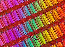 A Haswell wafer with several dies, with a pin for scale | |
| Launched | June 4, 2013; 10 years ago (June 4, 2013) |
|---|
| CPUID code | 0306C3h |
|---|
| Product code | |
|---|
|
| L1 cache | 64 KB per core |
|---|
| L2 cache | 256 KB per core |
|---|
| L3 cache | 2–45 MB (shared) |
|---|
| L4 cache | 128 MB of eDRAM (Iris Pro models only) |
|---|
|
| Technology node | 22 nm (Tri-Gate) |
|---|
| Microarchitecture | Haswell |
|---|
| Instruction set | x86-64 |
|---|
| Instructions | x86, x86-64 |
|---|
| Extensions | - AES-NI, CLMUL, RDRAND, TXT
- MMX, SSE, SSE2, SSE3, SSSE3, SSE4, SSE4.1, SSE4.2, FMA3, AVX, AVX2, and TSX (disabled via microcode, except for Haswell-EX)
- VT-x, VT-d
|
|---|
|
| Cores | - 2–4 (mainstream)
- 6–8 (enthusiast)
- 2–18 (Xeon)
|
|---|
| GPU(s) | - HD Graphics 4200
- HD Graphics 4400
- HD Graphics 4600
- HD Graphics 5000
- Iris 5100
- Iris Pro 5200
|
|---|
| Socket(s) | |
|---|
|
| Model(s) | - Haswell
- Haswell Refresh
- Haswell-E
- Haswell-EP
- Haswell-EX
|
|---|
| Brand name(s) | - Core i3
- Core i5
- Core i7
- Xeon E3 v3
- Xeon E5 v3
- Xeon E7 v3
- Pentium
- Celeron
|
|---|
|
| Predecessor | Sandy Bridge (Tock)
Ivy Bridge (Tick) |
|---|
| Successor | Broadwell (Tick/Process)
Skylake (Tock) |
|---|
|
| Unsupported |
Broadwell|
| Launched | October 27, 2014; 9 years ago (October 27, 2014) |
|---|
| Discontinued | November 2018[8] |
|---|
| CPUID code | 0306D4h |
|---|
| Product code | - 80658 (mainstream desktop/mobile, Xeon E3)
- 80660 (Xeon E5)
- 80669 (Xeon E7)
- 80671 (enthusiast desktop)
- 80674 (Xeon D)
- 80682 (Xeon D, Hewitt Lake)
|
|---|
|
| L1 cache | 64 KB per core |
|---|
| L2 cache | 256 KB per core |
|---|
| L3 cache | 2-6 MB (shared) |
|---|
| L4 cache | 128 MB of eDRAM (Iris Pro models only) |
|---|
|
| Technology node | 14 nm (Tri-Gate) |
|---|
| Microarchitecture | Haswell |
|---|
| Instruction set | x86-64 |
|---|
| Instructions | x86, x86-64 |
|---|
| Extensions | - MMX, SSE, SSE2, SSE3, SSSE3, SSE4, SSE4.1, SSE4.2, AVX, AVX2, TSX, FMA3
- AES-NI, CLMUL, RDRAND, TXT
- VT-x, VT-d
|
|---|
|
| Cores | - 2–4 (mainstream)
- 6–10 (enthusiast)
- 4–24 (Xeon)
|
|---|
| GPU(s) | - HD 5300
- HD 5500
- HD 5700P
- HD 6000
- HD 6100
- HD 6200
- HD 6300P
- HD Graphics
|
|---|
| Socket(s) | |
|---|
|
| Brand name(s) | |
|---|
|
| Predecessor | |
|---|
| Successor | Skylake (Tock/Architecture) |
|---|
|
| Unsupported |
Skylake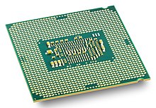 Intel Core i7-6700K with four physical cores | |
| Launched | August 5, 2015; 8 years ago (August 5, 2015) |
|---|
| Discontinued | March 4, 2019; 5 years ago (March 4, 2019) (desktop processors) |
|---|
| Marketed by | Intel |
|---|
| Designed by | Intel |
|---|
| Common manufacturer(s) | |
|---|
| CPUID code | 0406e3h, 0506e3h |
|---|
| Product code | - 80662 (mainstream and mobile Xeon E3)
- 80673 (enthusiast and server)
|
|---|
|
| Max. CPU clock rate | Up to 4.5 GHz |
|---|
|
| L1 cache | 64 KB per core |
|---|
| L2 cache | 256 KB per core
(1 MB per core for Skylake-X) |
|---|
| L3 cache | Up to 2 MB per core
(1.375 MB per core for Skylake-X) |
|---|
| L4 cache | 128 MB of eDRAM (on select models) |
|---|
|
| Technology node | 14 nm bulk silicon 3D transistors (Tri-Gate) |
|---|
| Microarchitecture | Skylake |
|---|
| Instruction set | x86-64 |
|---|
| Instructions | x86-64 (Intel 64) |
|---|
| Extensions | - AES-NI, CLMUL, RDRAND, MPX, TXT, SGX[9]
- MMX, SSE, SSE2, SSE3, SSSE3, SSE4, SSE4.1, SSE4.2, ADX
- AVX, AVX2, AVX-512 (SkyLake-SP, SkyLake-W & SkyLake-X[10]), TSX, FMA3
- VT-x, VT-d
|
|---|
|
| Cores | |
|---|
| Socket(s) | - Desktop
- Server & Workstation
- Mobile
- BGA 1168
- BGA 1356
- BGA 1515
- BGA 1440[11]
|
|---|
|
| Brand name(s) | - Core i3
- Core i5
- Core i7
- Core i9
- Core m3
- Core m5
- Core m7
- Xeon
- Celeron
- Pentium
|
|---|
|
| Predecessor | Broadwell (Tick/Process) |
|---|
| Successor | |
|---|
|
Client: Legacy support for iGPU
Xeon E3: Legacy support for iGPU
Other Xeon: supported |
Cannon Lake|
| Launched | May 15, 2018; 5 years ago (May 15, 2018) |
|---|
| Discontinued | February 28, 2020; 4 years ago (February 28, 2020) |
|---|
| Marketed by | Intel |
|---|
| Designed by | Intel |
|---|
| Common manufacturer(s) | |
|---|
|
| Max. CPU clock rate | 3.2 GHz |
|---|
|
| L1 cache | 64 KB per core |
|---|
| L2 cache | 256 KB per core |
|---|
| L3 cache | 2 MB per core |
|---|
|
| Technology node | Intel 10 nm (tri-gate) transistors |
|---|
| Microarchitecture | Palm Cove |
|---|
| Instruction set | x86-64 |
|---|
| Instructions | x86-64, Intel 64 |
|---|
| Extensions | - MMX, AES-NI, CLMUL, RDRAND, FMA3, SSE, SSE2, SSE3, SSSE3, SSE4, SSE4.1, SSE4.2, AVX, AVX2, AVX-512, SHA,[12] TXT, TSX, SGX, VT-x, VT-d
|
|---|
|
| Cores | |
|---|
| GPU(s) | Factory disabled |
|---|
| Socket(s) | |
|---|
|
| Brand name(s) | |
|---|
|
| Predecessor | Desktop: Coffee Lake (2nd optimization)
Kaby Lake Refresh (2nd optimization) |
|---|
| Successor | Ice Lake (architecture) |
|---|
|
| Legacy support for iGPU |
|
Testing main template[edit]
{{Infobox CPU}}
P6 | |
| Launched | November 1, 1995; 28 years ago (November 1, 1995) |
|---|
|
| Max. CPU clock rate | 150[16] MHz to 1.40 GHz |
|---|
| FSB speeds | 66 MHz to 133 MHz |
|---|
|
| L1 cache | Pentium Pro: 16 KB (8 KB I cache + 8 KB D cache)
Pentium II/III: 32 KB (16 KB I cache + 16 KB D cache) |
|---|
| L2 cache | 128 KB to 512 KB
256 KB to 2048 KB (Xeon) |
|---|
|
| Microarchitecture | P6 |
|---|
| Instruction set | x86 |
|---|
| Extensions | - MMX (Pentium II/III)
SSE (Pentium III)
|
|---|
|
| Transistors | |
|---|
| Cores | |
|---|
| Socket(s) | |
|---|
|
| Model(s) | - Celeron Series
- Pentium II Series
- Pentium III Series
- Pentium Pro Series
- Pentium II Xeon Series
- Pentium III Xeon Series
|
|---|
| Variant(s) | - Pentium M
- Enhanced Pentium M
|
|---|
|
| Predecessor(s) | P5 |
|---|
| Successor(s) | NetBurst, Pentium M |
|---|
|
| Unsupported |
NetBurst|
| Launched | November 20, 2000; 23 years ago (November 20, 2000) |
|---|
|
| Max. CPU clock rate | 1.3 GHz to 3.8 GHz |
|---|
| FSB speeds | 400 MT/s to 1066 MT/s |
|---|
|
| L1 cache | 8 KB to 16 KB per core |
|---|
| L2 cache | 128 KB to 2048 KB |
|---|
| L3 cache | 4 MB to 16 MB shared |
|---|
|
| Microarchitecture | NetBurst |
|---|
| Instruction set | x86 (IA-32), x86-64 (some) |
|---|
| Extensions | |
|---|
|
| Transistors | - 42M 180 nm (B2, C1, D0, E0)
- 55M 130 nm (B0, C1, D1, M0)
- 125M 90 nm (C0, D0, E0, G1)
- 169M 90 nm (M0, N0, R0)
- 230M 90 nm (A0, B0)
- 188M 65 nm (B1, C1, D0)
- 376M 65 nm (B1, C1, D0)
- 1,328M 65 nm (B0)
|
|---|
| Cores | - 1-2 (2-4 threads with HT)
|
|---|
| Socket(s) | |
|---|
|
| Model(s) | - Celeron Series
- Celeron D Series
- Pentium 4 Series
- Pentium D Series
- Xeon Series
|
|---|
|
| Predecessor(s) | P6 |
|---|
| Successor(s) | Intel Core
IA-64 |
|---|
Sandy Bridge|
| Launched | January 9, 2011; 13 years ago (January 9, 2011) |
|---|
| Discontinued | September 27, 2013 [17] |
|---|
| Product code | 80619 (extreme desktop)
80620 (server LGA1356)
80621 (server LGA2011)
80623 (desktop)
80627 (mobile) |
|---|
|
| Max. CPU clock rate | 1.60 GHz to 3.60 GHz |
|---|
| DMI speeds | 5.00 GT/s GT/s |
|---|
|
| L1 cache | 64 KB per core |
|---|
| L2 cache | 256 KB per core |
|---|
| L3 cache | 1 MB to 8 MB shared
10 MB to 15 MB (Extreme)
3 MB to 20 MB (Xeon) |
|---|
|
| Microarchitecture | Sandy Bridge |
|---|
| Instruction set | x86-64 |
|---|
| Instructions | x86, x86-64 |
|---|
| Extensions | - MMX, SSE, SSE2, SSE3, SSSE3, SSE4, SSE4.1, SSE4.2, AVX
- VT-x, VT-d
- AES-NI, CLMUL, TXT
|
|---|
|
| Transistors | |
|---|
| Cores | - 1–4 (4-6 Extreme, 2-8 Xeon)
|
|---|
| GPU(s) | HD Graphics
650 MHz to 1100 MHz
HD Graphics 2000
650 MHz to 1250 MHz
HD Graphics 3000
650 MHz to 1350 MHz
HD Graphics P3000
850 MHz to 1350 MHz |
|---|
| Socket(s) | |
|---|
|
| Model(s) | |
|---|
|
| Predecessor(s) | Nehalem (Tock)
Westmere (Tick) |
|---|
| Successor(s) | Ivy Bridge (Tick)
Haswell (Tock) |
|---|
|
| Unsupported |
Ivy BridgeIntel's internal Ivy Bridge logo [18] | |
| Launched | April 29, 2012; 12 years ago (April 29, 2012) |
|---|
| Discontinued | June 5, 2015; 8 years ago (June 5, 2015) |
|---|
| Marketed by | Intel |
|---|
| Designed by | Intel |
|---|
| Common manufacturer(s) | |
|---|
| CPUID code | 0306A9h |
|---|
| Product code | 80633 (extreme desktop)
80634 (server LGA1356)
80635 (server E5 LGA2011)
80636 (server E7 LGA2011)
80637 (desktop)
80638 (mobile) |
|---|
|
| Max. CPU clock rate | 1.4 to 4.1 GHz |
|---|
| DMI speeds | 5.00 GT/s |
|---|
|
| L1 cache | 64 KB per core |
|---|
| L2 cache | 256 KB per core |
|---|
| L3 cache | 2 to 8 MB shared |
|---|
|
| Technology node | Intel 22 nm |
|---|
| Microarchitecture | Sandy Bridge |
|---|
| Instruction set | x86-64 |
|---|
| Instructions | x86, x86-64 |
|---|
| Extensions | - MMX, SSE, SSE2, SSE3, SSSE3, SSE4, SSE4.1, SSE4.2, AVX, F16C
- AES-NI, CLMUL, RDRAND, TXT
- VT-x, VT-d
|
|---|
|
| Transistors | |
|---|
| Cores | - 2–4 (Mainstream)
2–15 (Xeon)
|
|---|
| GPU(s) | HD Graphics 2500
650 to 1150 MHz
HD Graphics 4000
350 to 1300 MHz
HD Graphics P4000
650 to 1250 MHz |
|---|
| Socket(s) | - Desktop & Workstation
- Server
- Mobile
|
|---|
|
| Model(s) | |
|---|
| Brand name(s) | |
|---|
|
| Predecessor(s) | Sandy Bridge (Tock) |
|---|
| Successor(s) | Haswell (Tock/Architecture) |
|---|
|
| Unsupported |
HaswellA Haswell wafer with several dies, with a pin for scale | |
| Launched | June 4, 2013; 10 years ago (June 4, 2013) |
|---|
| CPUID code | 0306C3h |
|---|
| Product code | |
|---|
|
| L1 cache | 64 KB per core |
|---|
| L2 cache | 256 KB per core |
|---|
| L3 cache | 2–45 MB (shared) |
|---|
| L4 cache | 128 MB of eDRAM (Iris Pro models only) |
|---|
|
| Technology node | 22 nm (Tri-Gate) |
|---|
| Microarchitecture | Haswell |
|---|
| Instruction set | x86-64 |
|---|
| Instructions | x86, x86-64 |
|---|
| Extensions | - AES-NI, CLMUL, RDRAND, TXT
- MMX, SSE, SSE2, SSE3, SSSE3, SSE4, SSE4.1, SSE4.2, FMA3, AVX, AVX2, and TSX (disabled via microcode, except for Haswell-EX)
- VT-x, VT-d
|
|---|
|
| Cores | - 2–4 (mainstream)
- 6–8 (enthusiast)
- 2–18 (Xeon)
|
|---|
| GPU(s) | - HD Graphics 4200
- HD Graphics 4400
- HD Graphics 4600
- HD Graphics 5000
- Iris 5100
- Iris Pro 5200
|
|---|
| Socket(s) | |
|---|
|
| Model(s) | - Haswell
- Haswell Refresh
- Haswell-E
- Haswell-EP
- Haswell-EX
|
|---|
| Brand name(s) | - Core i3
- Core i5
- Core i7
- Xeon E3 v3
- Xeon E5 v3
- Xeon E7 v3
- Pentium
- Celeron
|
|---|
|
| Predecessor(s) | Sandy Bridge (Tock)
Ivy Bridge (Tick) |
|---|
| Successor(s) | Broadwell (Tick/Process)
Skylake (Tock) |
|---|
|
| Unsupported |
Broadwell|
| Launched | October 27, 2014; 9 years ago (October 27, 2014) |
|---|
| Discontinued | November 2018[19] |
|---|
| CPUID code | 0306D4h |
|---|
| Product code | - 80658 (mainstream desktop/mobile, Xeon E3)
- 80660 (Xeon E5)
- 80669 (Xeon E7)
- 80671 (enthusiast desktop)
- 80674 (Xeon D)
- 80682 (Xeon D, Hewitt Lake)
|
|---|
|
| L1 cache | 64 KB per core |
|---|
| L2 cache | 256 KB per core |
|---|
| L3 cache | 2-6 MB (shared) |
|---|
| L4 cache | 128 MB of eDRAM (Iris Pro models only) |
|---|
|
| Technology node | 14 nm (Tri-Gate) |
|---|
| Microarchitecture | Haswell |
|---|
| Instruction set | x86-64 |
|---|
| Instructions | x86, x86-64 |
|---|
| Extensions | - MMX, SSE, SSE2, SSE3, SSSE3, SSE4, SSE4.1, SSE4.2, AVX, AVX2, TSX, FMA3
- AES-NI, CLMUL, RDRAND, TXT
- VT-x, VT-d
|
|---|
|
| Cores | - 2–4 (mainstream)
- 6–10 (enthusiast)
- 4–24 (Xeon)
|
|---|
| GPU(s) | - HD 5300
- HD 5500
- HD 5700P
- HD 6000
- HD 6100
- HD 6200
- HD 6300P
- HD Graphics
|
|---|
| Socket(s) | |
|---|
|
| Brand name(s) | |
|---|
|
| Predecessor(s) | |
|---|
| Successor(s) | Skylake (Tock/Architecture) |
|---|
|
| Unsupported |
SkylakeIntel Core i7-6700K with four physical cores | |
| Launched | August 5, 2015; 8 years ago (August 5, 2015) |
|---|
| Discontinued | March 4, 2019; 5 years ago (March 4, 2019) (desktop processors) |
|---|
| Marketed by | Intel |
|---|
| Designed by | Intel |
|---|
| Common manufacturer(s) | |
|---|
| CPUID code | 0406e3h, 0506e3h |
|---|
| Product code | - 80662 (mainstream and mobile Xeon E3)
- 80673 (enthusiast and server)
|
|---|
|
| Max. CPU clock rate | Up to 4.5 GHz |
|---|
|
| L1 cache | 64 KB per core |
|---|
| L2 cache | 256 KB per core
(1 MB per core for Skylake-X) |
|---|
| L3 cache | Up to 2 MB per core
(1.375 MB per core for Skylake-X) |
|---|
| L4 cache | 128 MB of eDRAM (on select models) |
|---|
|
| Technology node | 14 nm bulk silicon 3D transistors (Tri-Gate) |
|---|
| Microarchitecture | Skylake |
|---|
| Instruction set | x86-64 |
|---|
| Instructions | x86-64 (Intel 64) |
|---|
| Extensions | - AES-NI, CLMUL, RDRAND, MPX, TXT, SGX[9]
- MMX, SSE, SSE2, SSE3, SSSE3, SSE4, SSE4.1, SSE4.2, ADX
- AVX, AVX2, AVX-512 (SkyLake-SP, SkyLake-W & SkyLake-X[10]), TSX, FMA3
- VT-x, VT-d
|
|---|
|
| Cores | |
|---|
| Socket(s) | - Desktop
- Server & Workstation
- Mobile
- BGA 1168
- BGA 1356
- BGA 1515
- BGA 1440[20]
|
|---|
|
| Brand name(s) | - Core i3
- Core i5
- Core i7
- Core i9
- Core m3
- Core m5
- Core m7
- Xeon
- Celeron
- Pentium
|
|---|
|
| Predecessor(s) | Broadwell (Tick/Process) |
|---|
| Successor(s) | |
|---|
|
Client: Legacy support for iGPU
Xeon E3: Legacy support for iGPU
Other Xeon: supported |
Cannon Lake|
| Launched | May 15, 2018; 5 years ago (May 15, 2018) |
|---|
| Discontinued | February 28, 2020; 4 years ago (February 28, 2020) |
|---|
| Marketed by | Intel |
|---|
| Designed by | Intel |
|---|
| Common manufacturer(s) | |
|---|
|
| Max. CPU clock rate | 3.2 GHz |
|---|
|
| L1 cache | 64 KB per core |
|---|
| L2 cache | 256 KB per core |
|---|
| L3 cache | 2 MB per core |
|---|
|
| Technology node | Intel 10 nm (tri-gate) transistors |
|---|
| Microarchitecture | Palm Cove |
|---|
| Instruction set | x86-64 |
|---|
| Instructions | x86-64, Intel 64 |
|---|
| Extensions | - MMX, AES-NI, CLMUL, RDRAND, FMA3, SSE, SSE2, SSE3, SSSE3, SSE4, SSE4.1, SSE4.2, AVX, AVX2, AVX-512, SHA,[12] TXT, TSX, SGX, VT-x, VT-d
|
|---|
|
| Cores | |
|---|
| GPU(s) | Factory disabled |
|---|
| Socket(s) | |
|---|
|
| Brand name(s) | |
|---|
|
| Predecessor(s) | Desktop: Coffee Lake (2nd optimization)
Kaby Lake Refresh (2nd optimization) |
|---|
| Successor(s) | Ice Lake (architecture) |
|---|
|
| Legacy support for iGPU |
|


.jpg)


