Apple A7
 The A7 processor | |
| General information | |
|---|---|
| Launched | September 20, 2013 |
| Discontinued | March 21, 2017 |
| Designed by | Apple Inc. |
| Common manufacturer | |
| Product code | S5L8960X[2][3] |
| Performance | |
| Max. CPU clock rate | 1.3 GHz[4] to 1.4 GHz[5] |
| Cache | |
| L1 cache | Per core: 64 KB instruction + 64 KB data[6] |
| L2 cache | 1 MB shared[6] |
| L3 cache | 4 MB[5] |
| Architecture and classification | |
| Application | Mobile |
| Technology node | 28 nm[1] |
| Microarchitecture | Cyclone[6] |
| Instruction set | ARMv8-A:[7][8] A64, A32, T32 |
| Physical specifications | |
| Cores |
|
| GPU | PowerVR G6430 (quad-core)[9] |
| History | |
| Predecessor | Apple A6 |
| Successor | Apple A8 |
The Apple A7 is a 64-bit system on a chip (SoC) designed by Apple Inc. It first appeared in the iPhone 5S, which was announced on September 10, 2013, and the iPad Air and iPad Mini 2, which were both announced on October 22, 2013. Apple states that it is up to twice as fast and has up to twice the graphics power compared to its predecessor, the Apple A6.[10] It is the first 64-bit SoC to ship in a consumer smartphone or tablet computer.[11] The latest software update for systems using this chip was iOS 12.5.5, released on September 23, 2021.
Design
The A7 features an Apple-designed[4] 64-bit[7] 1.3[4]–1.4[5] GHz ARMv8-A[6][8] dual-core CPU,[4] called Cyclone.[6] The 64-bit A64 instruction set in the ARMv8-A architecture doubles the number of registers of the A7 compared to the ARMv7 architecture used in A6.[12] It has 31 general purpose registers that are each 64-bits wide and 32 floating-point/NEON registers that are each 128-bits wide.[7]
The A7 also integrates a graphics processing unit (GPU) which AnandTech believes to be a PowerVR G6430 in a four cluster configuration.[9]
The A7 has a per-core L1 cache of 64 KB for data and 64 KB for instructions, a L2 cache of 1 MB shared by both CPU cores,[6] and a 4 MB L3 cache that services the entire SoC.[5]
The A7 includes a new image processor, a feature originally introduced in the A5, used for functionality related to the camera such as image stabilizing, color correction, and light balance.[13][14] The A7 also includes an area called the "Secure Enclave" that stores and protects the data from the Touch ID fingerprint sensor on the iPhone 5S and iPad mini 3.[10] It has been speculated that the security of the data in the Secure Enclave is enforced by ARM's TrustZone/SecurCore technology.[15] In a change from the Apple A6, the A7 SoC no longer services the accelerometer, gyroscope and compass. In order to reduce power consumption, this functionality has been moved to the new M7 motion coprocessor[16][17] which appears to be a separate ARM-based microcontroller from NXP Semiconductors.[1]
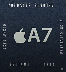
Apple A7 (APL0698)
Apple uses the APL0698 variant of the A7 chip, running at 1.3 GHz,[4] in the iPhone 5S, iPad Mini 2, and iPad Mini 3.[18] This A7 is manufactured by Samsung on a high-κ metal gate (HKMG) 28 nm process[1][19] and the chip includes over 1 billion transistors on a die 102 mm2 in size.[4] According to ABI Research the A7 drew 1100 mA during fixed point operations and 520 mA during floating point operations, while its predecessor, the A6 processor in the iPhone 5, drew 485 mA and 320 mA.[20] It is manufactured in a package on package (PoP) together with 1 GB of LPDDR3 DRAM with a 64-bit wide memory interface onto the package.[6][21]
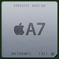
Apple A7 (APL5698)
Apple uses the APL5698 variant of the A7 chip, running at 1.4 GHz,[5] in the iPad Air. Its die is identical in size and layout to that of the first A7 and is manufactured by Samsung.[22] However, unlike the first version of the A7, the A7 used in the iPad Air is not on a PoP, having no stacked RAM. Instead it uses a chip-on-board mounting, immediately adjacent DRAM, and is covered by a metallic heat spreader, similar to the Apple A5X and A6X.[22][23]
Patent litigation
The A7's branch predictor was claimed to infringe on a 1998 patent.[24] On October 14, 2015, a district judge found Apple guilty of infringing U.S. patent US 5781752, "Table based data speculation circuit for parallel processing computer", on the Apple A7 and A8 processors.[25] The patent is owned by Wisconsin Alumni Research Foundation (WARF), a firm affiliated with the University of Wisconsin. On July 24, 2017, Apple was ordered to pay WARF $506 million for patent infringement. Apple filed an appellate brief on October 26, 2017 with the U.S. Court of Appeals for the Federal Circuit, that argued that Apple did not infringe on the patent owned by the Wisconsin Alumni Research Foundation.[26] On September 28, 2018, the ruling was overturned on appeal and the award thrown out by the U.S. Federal Circuit Court of Appeals.[27] The patent expired in December 2016.[28]
Products that include the Apple A7
Gallery
These images are illustrations only.
See also
- Apple silicon, the range of ARM-based processors designed by Apple.
- Comparison of ARMv8-A cores
References
- ^ a b c d Tanner, Jason; Morrison, Jim; James, Dick; Fontaine, Ray; Gamache, Phil (September 20, 2013). "Inside the iPhone 5s". Chipworks. Archived from the original on August 3, 2014. Retrieved September 20, 2013.
- ^ Gurman, Mark (July 31, 2013). "Apple's upcoming A7 iPhone chip will have Samsung components, code inside iOS 7 reveals". 9to5Mac. Retrieved September 13, 2013.
- ^ Klug, Brian (October 24, 2013). "iPad Air and iPad Mini with Retina Display include Qualcomm's MDM9615 baseband". AnandTech. Retrieved November 17, 2013.
It isn't news, but I've also confirmed that there are the appropriate references to Apple's S5L8960X SoC (otherwise known as Apple's A7) in the iPad Air and iPad mini with Retina Display software bundles, same as the iPhone 5s.
- ^ a b c d e f g Lal Shimpi, Anand (September 17, 2013). "The iPhone 5s Review: A7 SoC Explained". AnandTech. Retrieved September 18, 2013.
- ^ a b c d e Lai Shimpi, Anand (October 29, 2013). "The iPad Air Review: iPhone to iPad: CPU Changes". AnandTech. Retrieved October 30, 2013.
- ^ a b c d e f g Lal Shimpi, Anand (September 17, 2013). "The iPhone 5s Review: After Swift Comes Cyclone". AnandTech. Retrieved September 18, 2013.
- ^ a b c Lal Shimpi, Anand (September 17, 2013). "The iPhone 5s Review: The Move to 64-bit". AnandTech. Retrieved September 18, 2013.
- ^ a b Lattner, Chris (September 10, 2013). "[LLVMdev] A7 processor support?". llvm-dev (Mailing list). Retrieved July 9, 2017.
- ^ a b Lal Shimpi, Anand (September 17, 2013). "The iPhone 5s Review: GPU Architecture". AnandTech. Retrieved September 18, 2013.
- ^ a b "Apple Announces iPhone 5s—The Most Forward-Thinking Smartphone in the World" (Press release). Apple. September 10, 2013. Retrieved September 13, 2013.
- ^ Lai Shimpi, Anand (September 10, 2013). "Apple Announces A7, World's First 64-bit Smartphone SoC". AnandTech. Retrieved September 16, 2013.
- ^ Cunningham, Andrew (September 10, 2013). "Apple unveils 64-bit iPhone 5S with fingerprint scanner, $199 for 16GB". Ars Technica. Retrieved September 12, 2013.
- ^ "iPhone 5s - Design". Apple. September 10, 2013. Retrieved September 13, 2013.
- ^ Panzarino, Matthew (September 12, 2013). "A Photographer's Take On The iPhone 5S Camera". TechCrunch. Retrieved September 13, 2013.
- ^ Mogull, Rich (September 23, 2013). "Investigating Touch ID and the Secure Enclave". Securosis. Retrieved September 25, 2013.
- ^ Lal Shimpi, Anand (September 17, 2013). "The iPhone 5s Review: M7 Motion Coprocessor". AnandTech. Retrieved September 18, 2013.
- ^ Lawler, Richard (September 10, 2013). "iPhone 5s packs M7 motion-sensing chip, CoreMotion API for more accurate tracking". Engadget. Retrieved September 11, 2013.
- ^ "iPad Mini Retina Display Teardown". IFixit. November 12, 2013.
- ^ "Chipworks Confirms Apple's A7 is Built On Samsung's 28nm HK+MG Process". AnandTech. Retrieved October 23, 2013.
- ^ Google/Motorola Mobility’s Moto X Outpaces Competition with New Innovations, ABI Research
- ^ "Quick Turn Teardown of the Apple iPhone 5s". TechInsights. September 20, 2013. Archived from the original on November 3, 2014. Retrieved September 20, 2013.
- ^ a b "Inside the iPad Air". Chipworks. November 1, 2013. Archived from the original on May 8, 2015. Retrieved November 13, 2013.
- ^ "iPad Air Teardown". IFixit. November 1, 2013.
- ^ Chirgwin, Richard (February 4, 2014). "Cupertino copied processor pipelining claims Wisconsin U". www.theregister.co.uk. The Register. Retrieved February 3, 2014.
- ^ Joe Mullin (October 14, 2015). "Apple faces $862M patent damage claim from University of Wisconsin". Ars Technica. Retrieved October 14, 2015.
- ^ Wolfe, Jan (October 26, 2017). "Apple urges appeals court to toss $506 million patent loss to WARF". Reuters. Retrieved February 22, 2018.
- ^ Stempel, Jonathan (September 28, 2018). "Apple wins reversal in University of Wisconsin patent lawsuit". Reuters. Retrieved November 17, 2018.
- ^ Wolfe, Jan (July 25, 2017). "Apple ordered to pay $506 million to university in patent dispute". Reuters. Retrieved July 26, 2017.


